Building Your Own Arduino
This chapter explains how to build a custom Arduino-compatible board. As projects grow, the original board's available pins and a single large program may become difficult to manage. A common solution is to divide a system among several MCUs: a motor module can handle driving and speed control, while an attitude sensor can calculate orientation. The main controller then communicates with those modules rather than performing every low-level task. LEGO robotics commonly uses for this; many newer educational robots use the more robust CAN bus.
1. What Is a Bootloader?
A bootloader is a small program that runs when a microcontroller starts. On an Arduino, it listens briefly for a new program arriving over the serial port, writes that program into flash memory, and then starts it. This is why a normal Arduino UNO can accept sketches over USB without using a separate hardware programmer every time.
Bare microcontrollers are normally programmed with tools such as an AVR ISP for the ATmega family or an ST-LINK for STM32 devices.
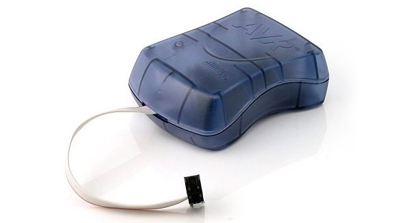
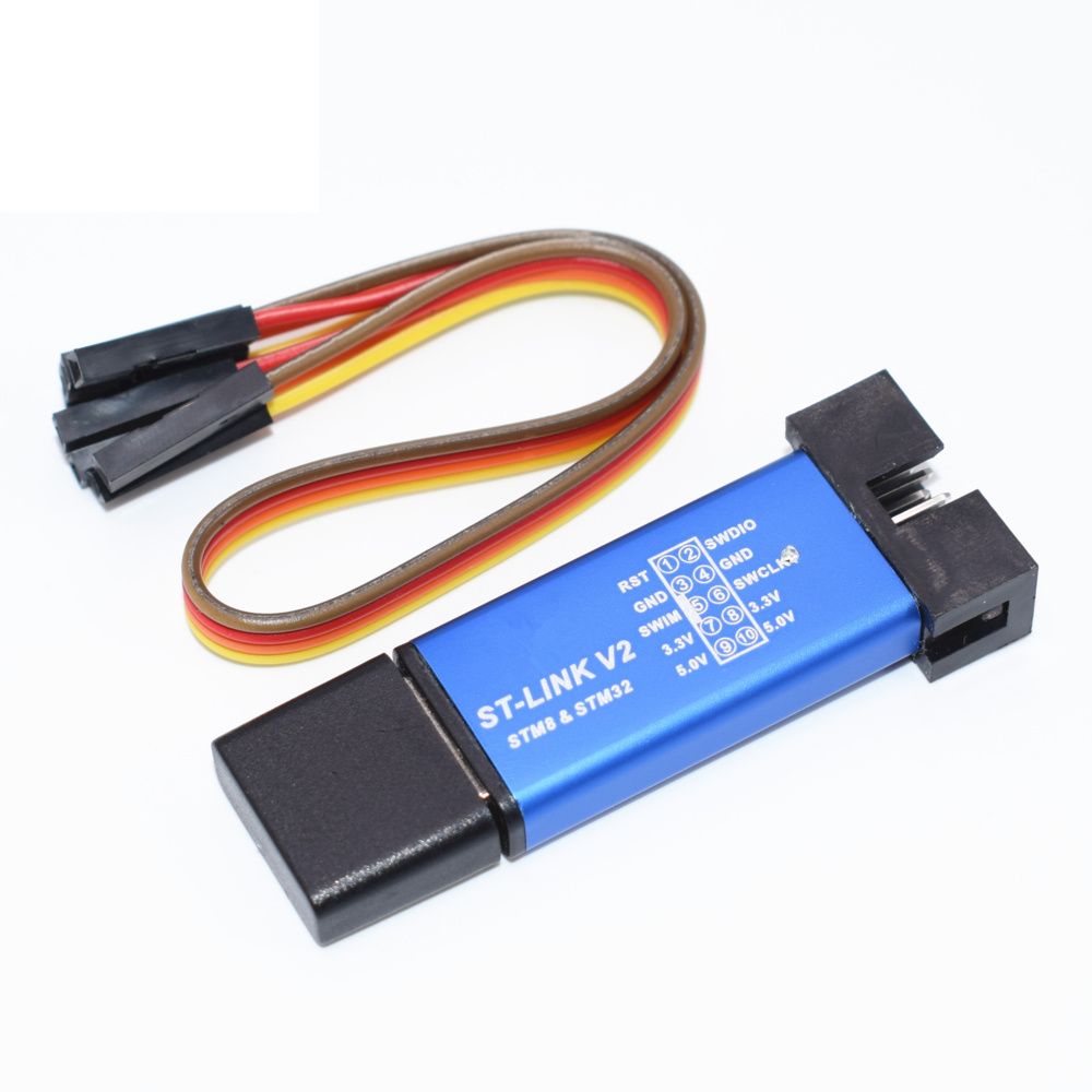
The UNO's ICSP header provides its direct programming connection.
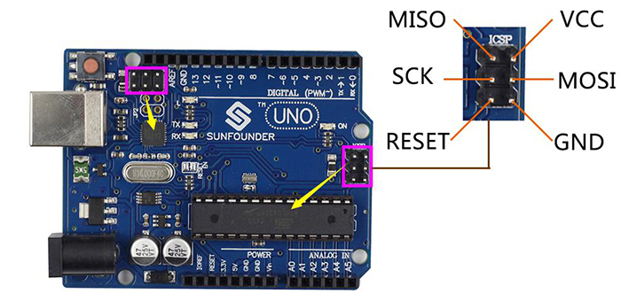
A custom Arduino-compatible board therefore needs either a pre-programmed bootloader or an accessible ICSP header through which the bootloader can be installed.
2. Burning the Bootloader
Possible methods include an AVR USBtinyISP, another AVR programmer, or another Arduino board. The third requires no additional programmer; see the official Arduino tutorial. The method below is adapted from Nick Gammon's guide, uses his board-programmer sketch, and also works conveniently with an unsoldered ATmega328.
Step 1
Upload Atmega_Board_Programmer to a working Arduino UNO.
Step 2
Connect that UNO to the target ATmega328:
Programmer UNO       Target ATmega328
D10 (SS)        -->  Reset
D11 (MOSI)      -->  D11 / MOSI
D12 (MISO)      -->  D12 / MISO
D13 (SCK)       -->  D13 / SCK
GND             -->  GND
+5V --> +5V| DIP-28 ATmega8/48/88/168/328 | TQFP-32 ATmega8/48/88/168/328 | TQFP-32 ATmega48/88/168/328PB |
|---|---|---|
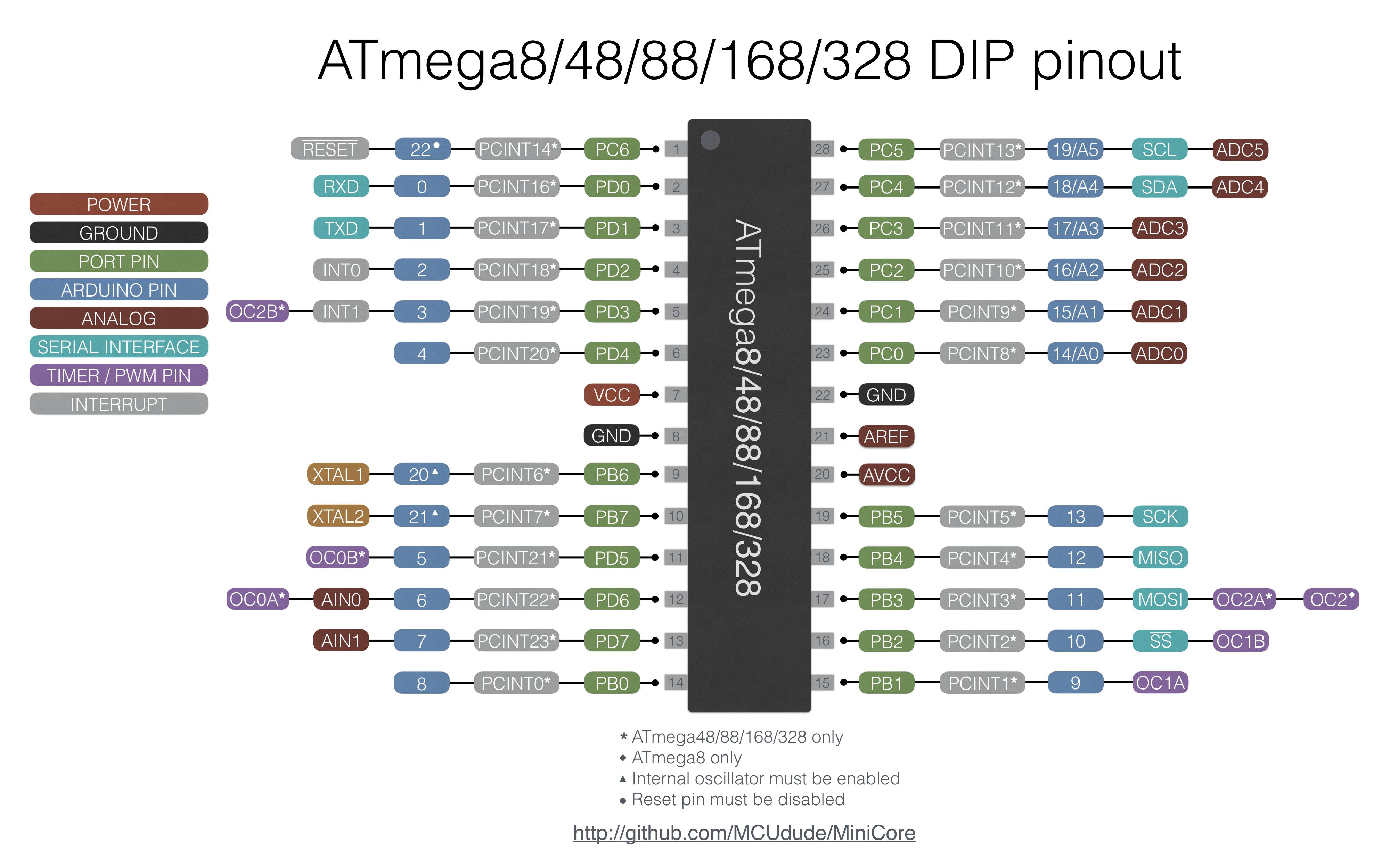 | 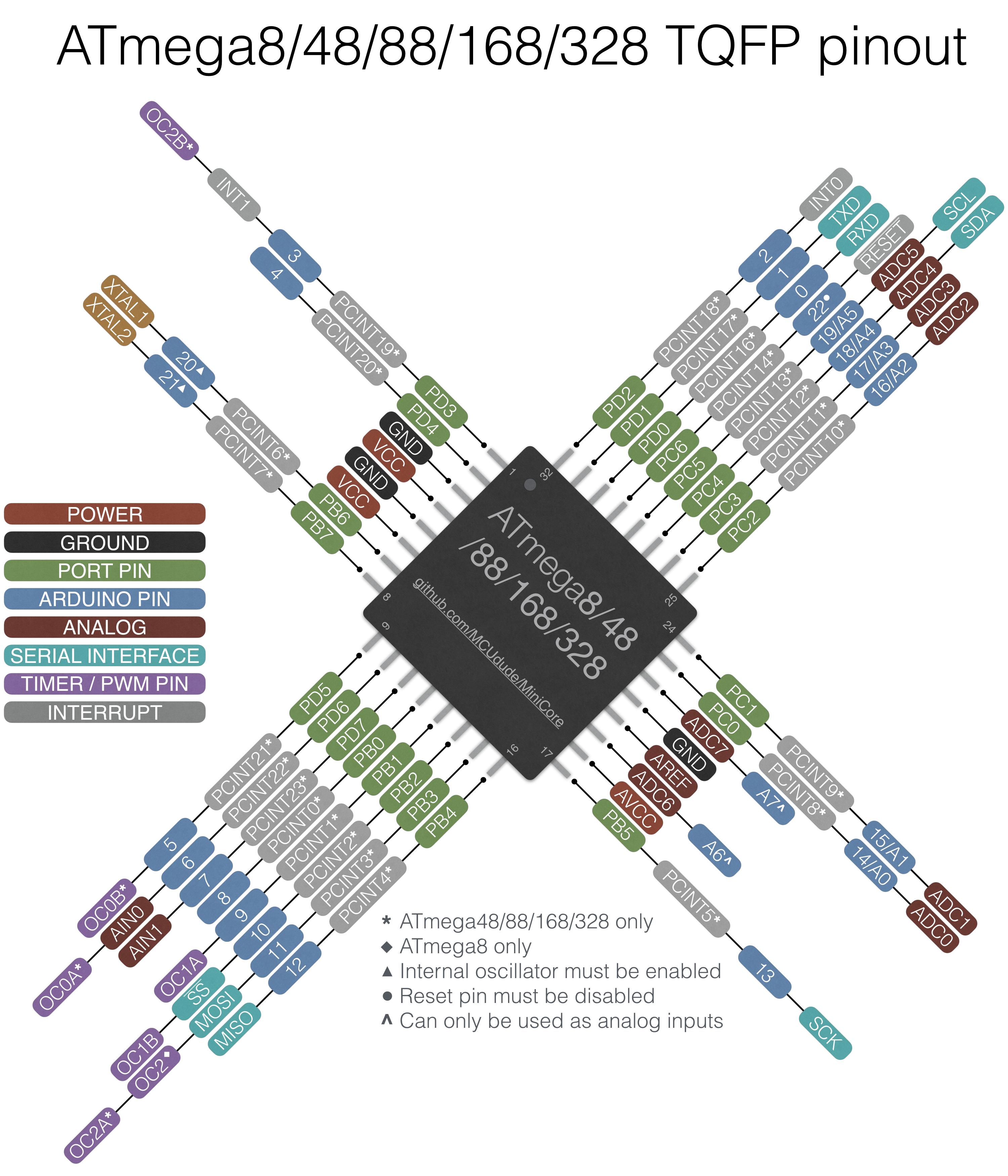 | 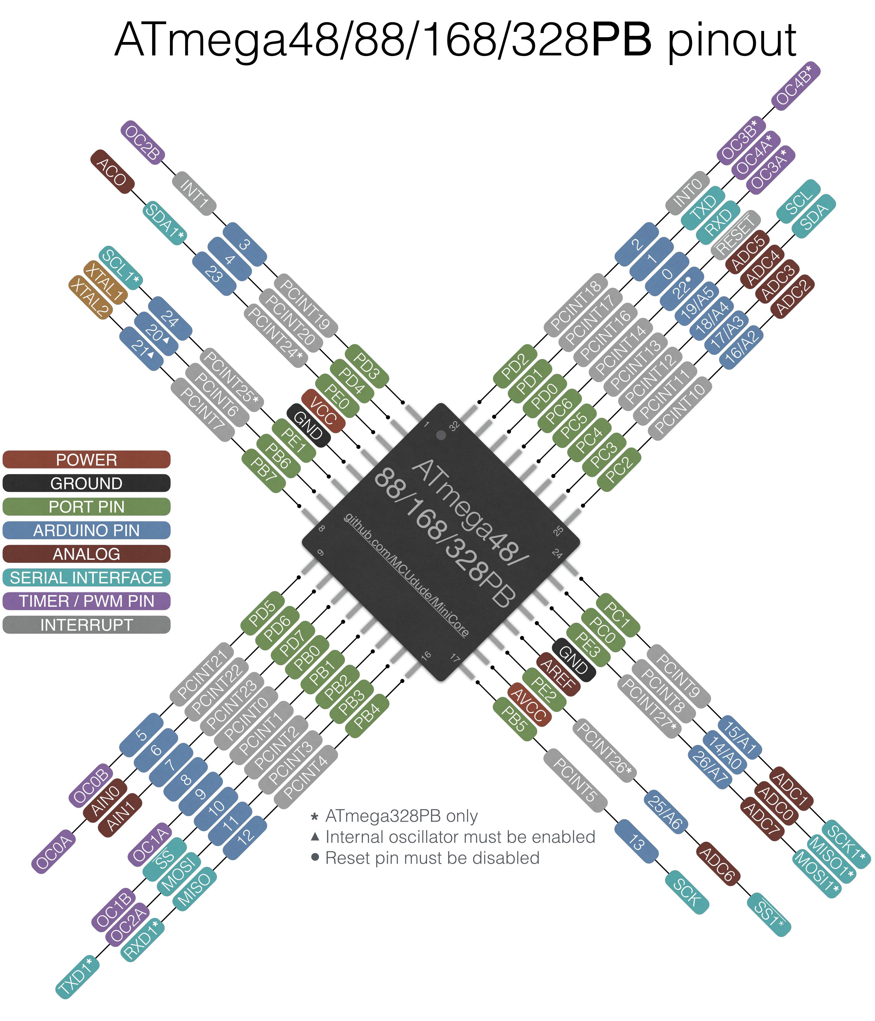 |
Use the pinout corresponding to your package to locate D11/MOSI, D12/MISO, D13/SCK, Reset, +5 V and GND.
Step 3
Open Serial Monitor. At the prompt, enter U for the UNO 16 MHz bootloader:
Type 'L' to use Lilypad (8 MHz) loader, or 'U' for Uno (16 MHz) loader ...If the wiring is correct, the programmer reports the target signature and fuse data. Enter G when prompted. It erases the chip, writes and verifies the bootloader, then writes the fuses. No errors found followed by Done confirms success.
3. Optional Dedicated Programmer
For repeated programming, a TQFP-32-to-DIP-32 adapter is convenient.
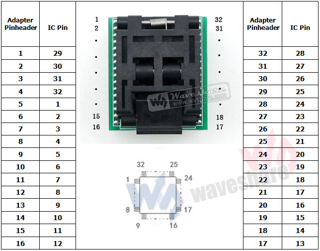
The following programmer was designed from the adapter mapping and the ATmega328/UNO pin assignments.
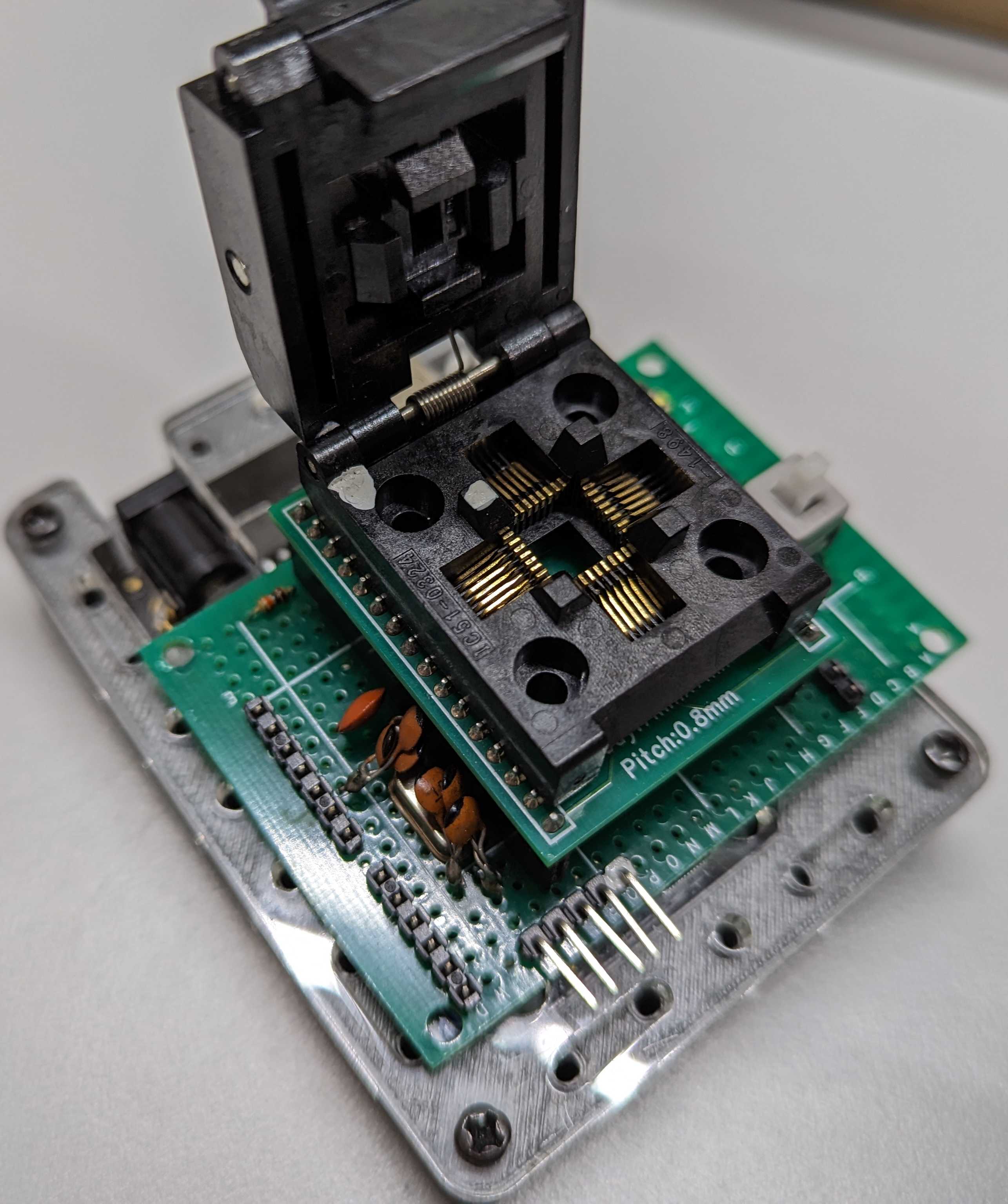
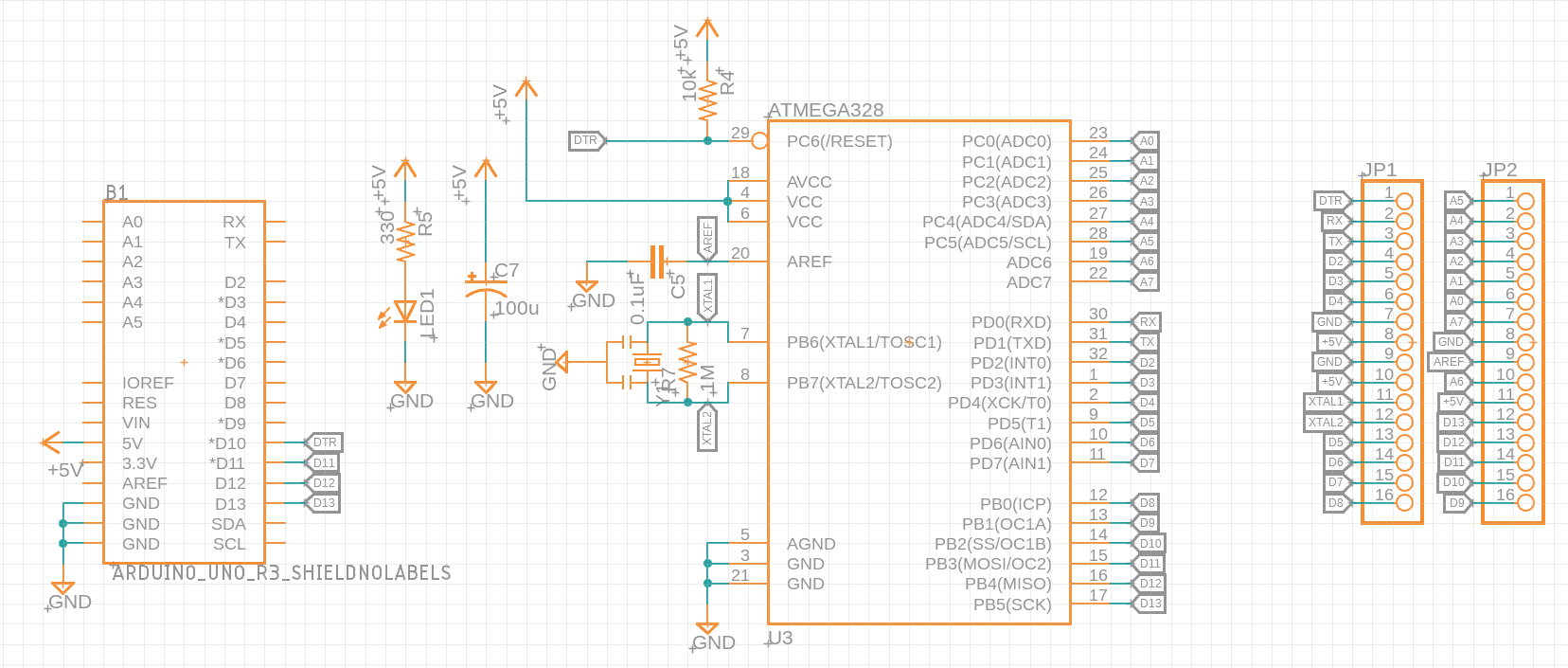
Because the target is a bare ATmega328 rather than a complete Arduino, it also needs the clock crystal, capacitors, reset resistor and other minimum-support parts.
An Arduino shield version makes the programmer easier to reuse.
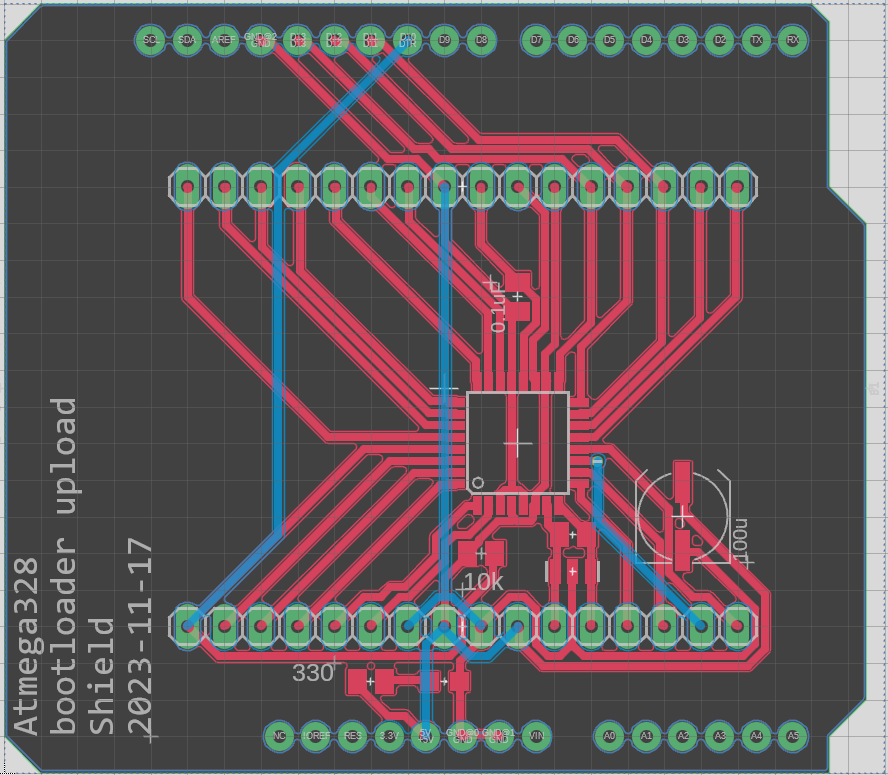
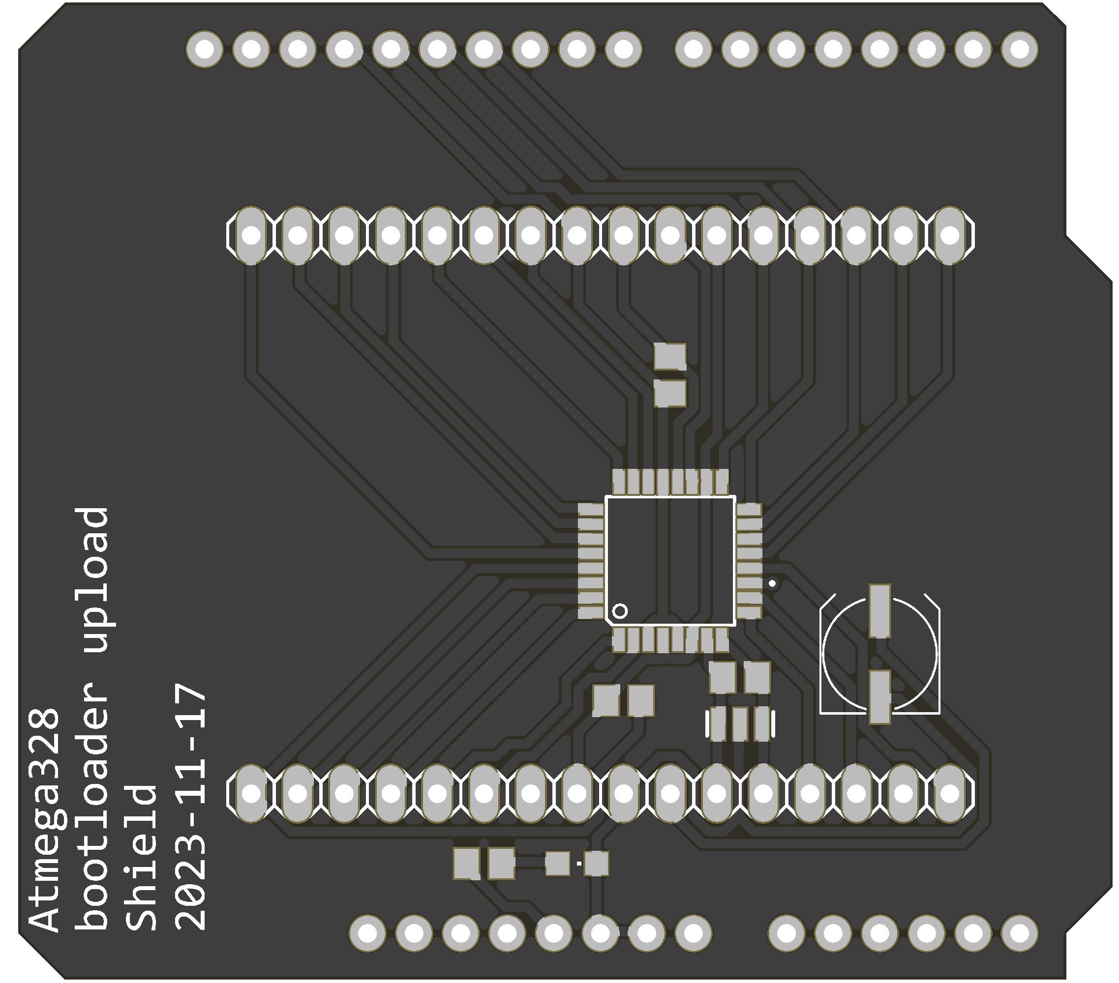
The shield supports both a TQFP socket adapter and exposed TQFP pads. For occasional programming, a chip can be held carefully against the pads without buying the adapter.
Download the Gerber production files.
4. Build the Arduino Board
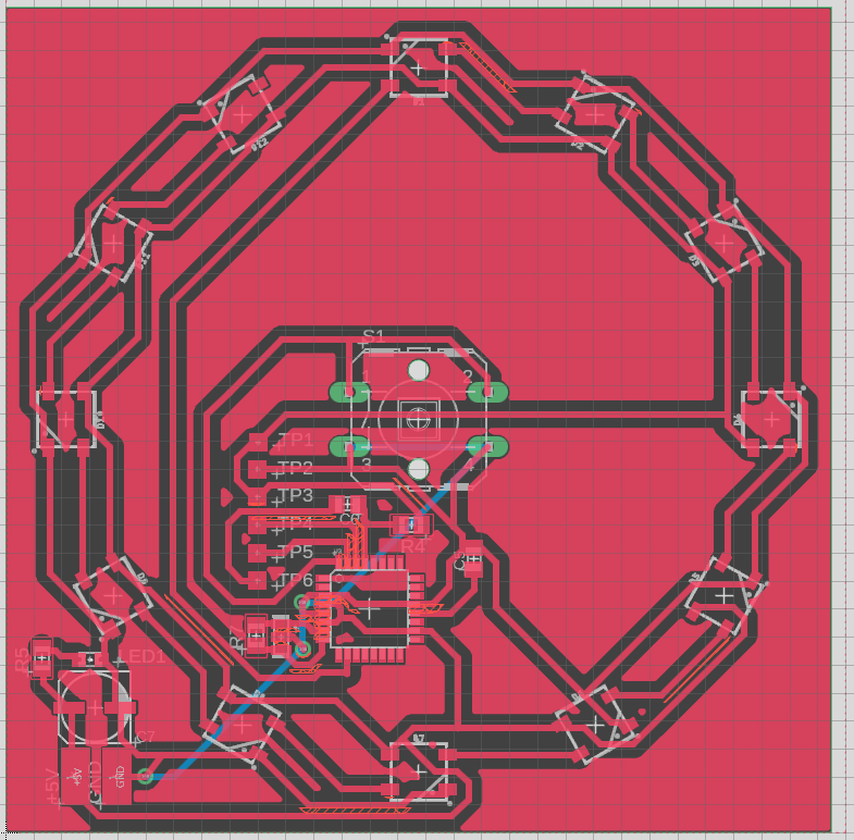
This project combines the previous home-made PCB process with a 12-pixel WS2812 ring. It can also be sent to a board manufacturer using the PCB manufacturing chapter.
4.1 Draw the Schematic
Reusable circuits can be stored as a Design Block. Download pro mini atmega328.dbl, which contains an Arduino Pro Mini-style ATmega328 circuit. A Pro Mini uses the same MCU as the UNO but omits the USB-to-serial interface; with a UNO bootloader it can still be programmed as an UNO through an external serial adapter.
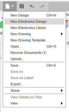
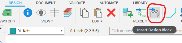
Create a New Electronics Design in Fusion 360 and use Insert Design Block to import it.
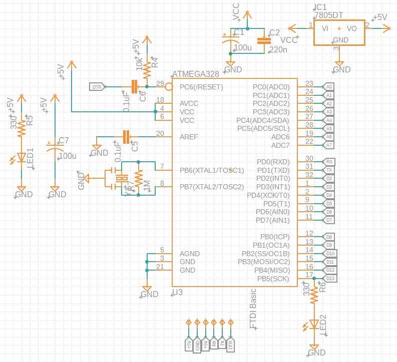
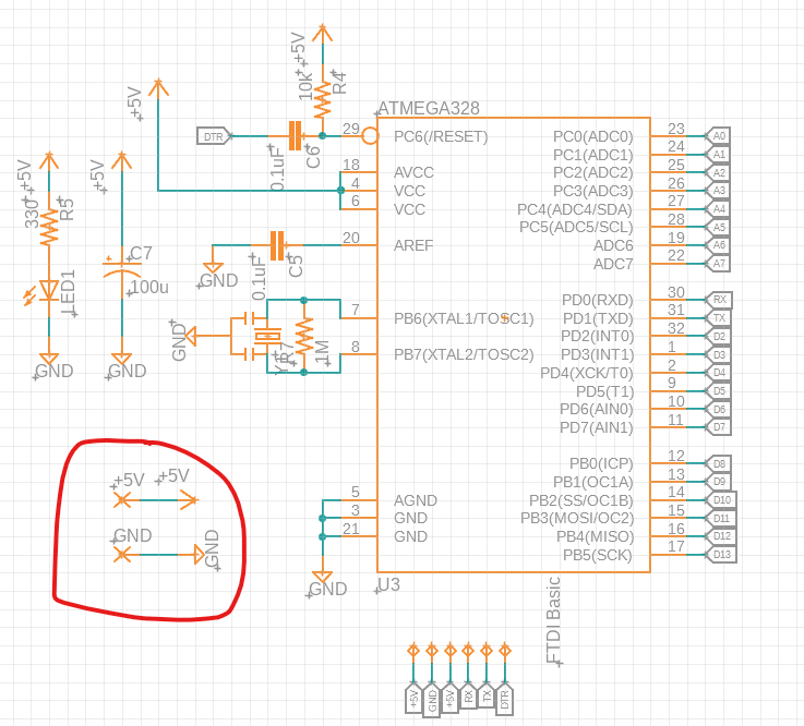
The block includes a 7805 regulator, pin-13 LED and decoupling capacitors. If the board receives regulated 5 V directly, remove the regulator section and built-in LED. Enter add, select SMD5 from the wirepad library and add +5 V and GND input pads.
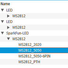
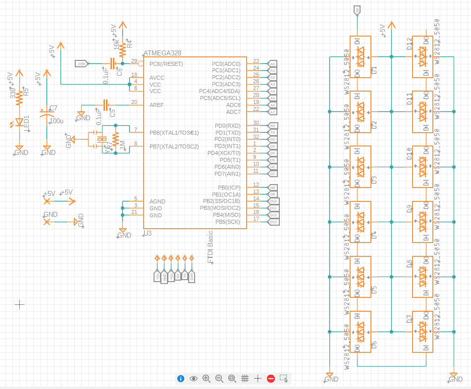
Add twelve WS2812_5050 parts from SparkFun-LED. Connect each DO to the next pixel's DI, connect power, and connect the first pixel's DI to Arduino D6.
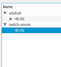
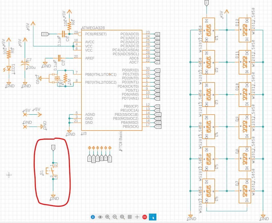
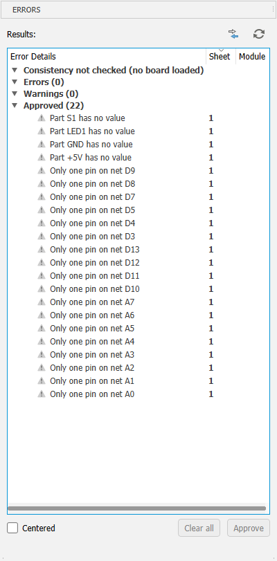
Add a 40-xx push-button to D2, run ERC and review/approve the expected warnings.
4.2 Design the PCB
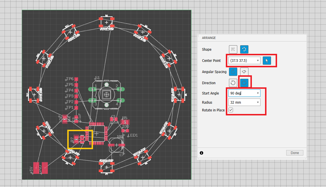
- Set the grid to millimetres with a
2.54 mmspacing. - Set the board outline to a
75 × 75 mmsquare. - Position the
40-xxbutton at(37.5, 37.5). - Select all twelve WS2812s and use
Arrangeto distribute them in a ring. - Place the other components while observing these rules:
- Keep crystal
Y1and resistorR7as close as possible to ATmega328 pins 7 and 8. - Place
TP1–TP6in a straight line at2.54 mm (100 mil)pitch for programming. - Put the +5 V and GND pads at a convenient corner.
- Plan the placement carefully to minimise vias.
- Keep crystal
- In DRC, use
0.5 mmtrack width,0.2 mmclearance and0.9 mmminimum drill. Route all ATmega328 pins manually while using the smaller clearance.
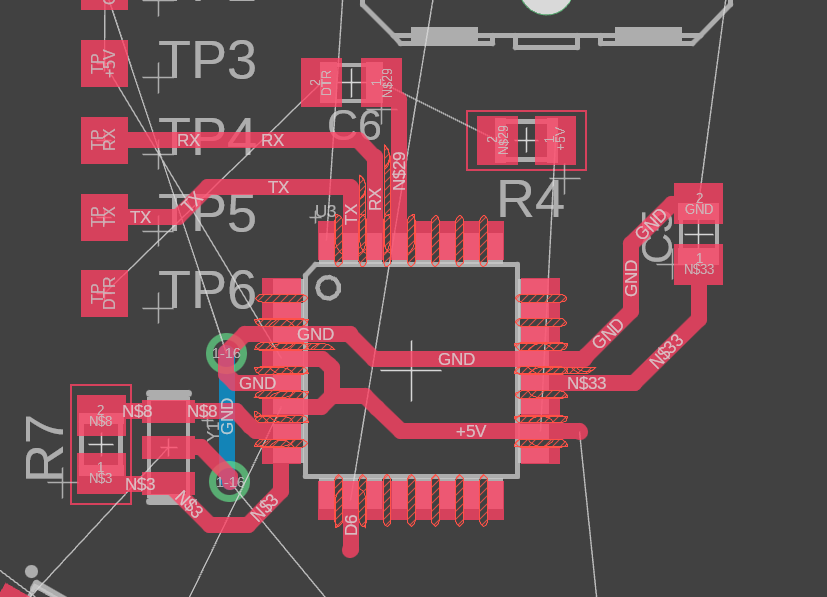
- Restore
0.5 mmclearance, then autoroute the remaining nets. Minimising vias may require rotating the WS2812s and rearranging the capacitors, indicator LED and test points. - Use
Showon +5 V and GND. Since the LED ring draws substantial current, add a via beside the GND input pad to provide a shorter return path to the ATmega328.
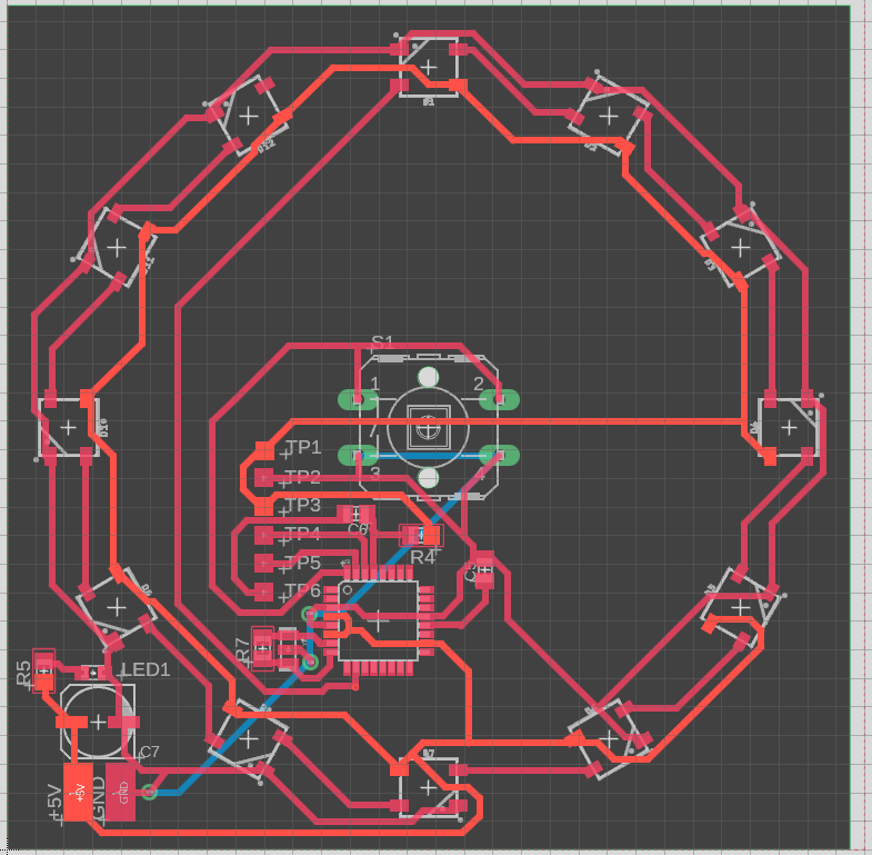
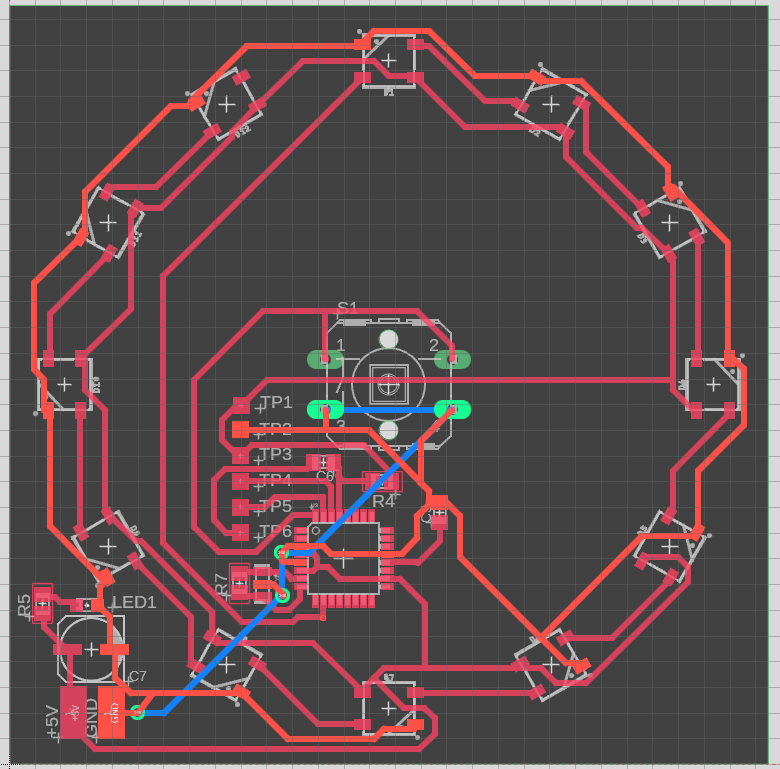
- Add the copper polygon, then set its clearance to
1 mmin DRC so that the home etching process is more reliable.
- Manufacture the PCB using the process in the previous chapter.
5. Upload a Program
Home etching this dense board has a relatively high failure rate, so professional manufacture is preferable where possible. Refer to Outsourcing PCB Production and the factory settings in Drawing Schematics and PCB Layouts. After soldering, upload a test program through an external USB-to-TTL adapter or a socketed UNO with its MCU removed.
5.1 FTDI USB-to-TTL Adapter
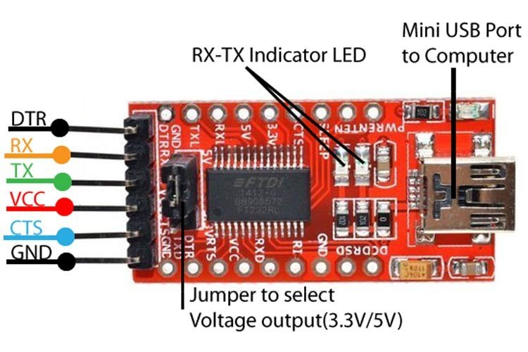
Connect the programming pads as follows:
Custom Arduino          Adapter
TP1  +5V          -->   not connected
TP2  GND          -->   GND
TP3  +5V          -->   +5V
TP4  RX           -->   TX
TP5  TX           -->   RX
TP6 DTR --> DTRThen upload as for a normal Arduino UNO.
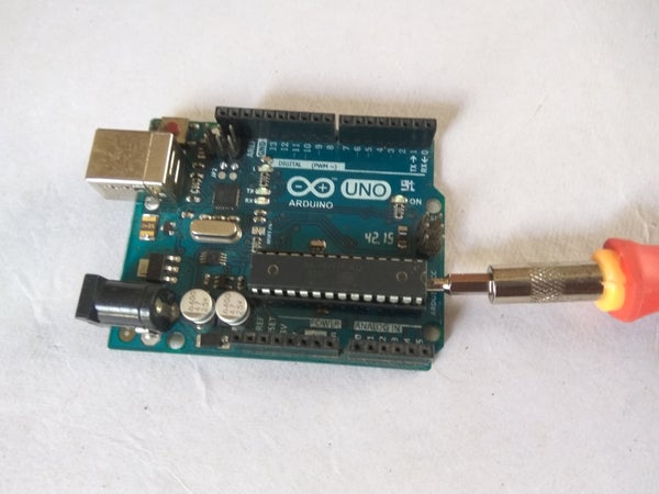
5.2 Socketed UNO with the MCU Removed
If no serial adapter is available, carefully remove the main IC from a socketed UNO with a flat screwdriver, taking care not to bend its pins.
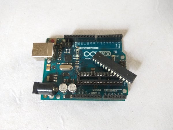
Custom Arduino          UNO without MCU
TP1  +5V          -->   not connected
TP2  GND          -->   GND
TP3  +5V          -->   +5V
TP4  RX           -->   RX (0)
TP5  TX           -->   TX (1)
TP6 DTR --> RESETUpload using the normal UNO workflow.
Translation notice: This English page was generated automatically by AI and has not yet been reviewed by a human. It will be checked and revised page by page when time permits.