Ordering PCB Manufacturing
This example uses JLCPCB, a service commonly seen in maker videos, because it is based in Shenzhen, ships quickly, accepts orders as small as five boards, and provides interactive options with instant pricing. PCB prices include setup and area costs, so ordering 50 boards does not necessarily cost exactly five times as much as ordering 10.
The website, prices and options may change after this article is written. This is an independent tutorial and not a paid promotion.
Export Manufacturing Files
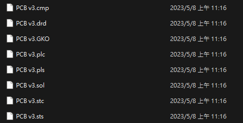
After checking the design and positioning all value/name labels, export the files for manufacturing. PCB factories accept a standard set of Gerber and drill files. This workflow produces eight files:
*.GKO— mechanical outline and milling paths (20: Dimension,48: Milling).*.CMP— component-side copper, pads and vias (1: Top,17: Pads,18: Vias).*.SOL— solder-side copper, pads and vias (16: Bottom,17: Pads,18: Vias).*.PLC— top silkscreen. The basic set uses20 Dimension,21 tPlaceand25 tNames; add27 tValueand51 tDocwhere useful.*.PLS— bottom silkscreen, using20 Dimension,22 bPlaceand26 bNames, optionally28 bValueand52 bDoc.*.STC— top solder-mask openings (29 tStop). This layer may also be used to make a solder-paste stencil.*.STS— bottom solder-mask openings (30 bStop).*.DRD— drill data (44 Drills,45 Holesand additionally46 Milling).
The CAM job shown below generates these manufacturing outputs.
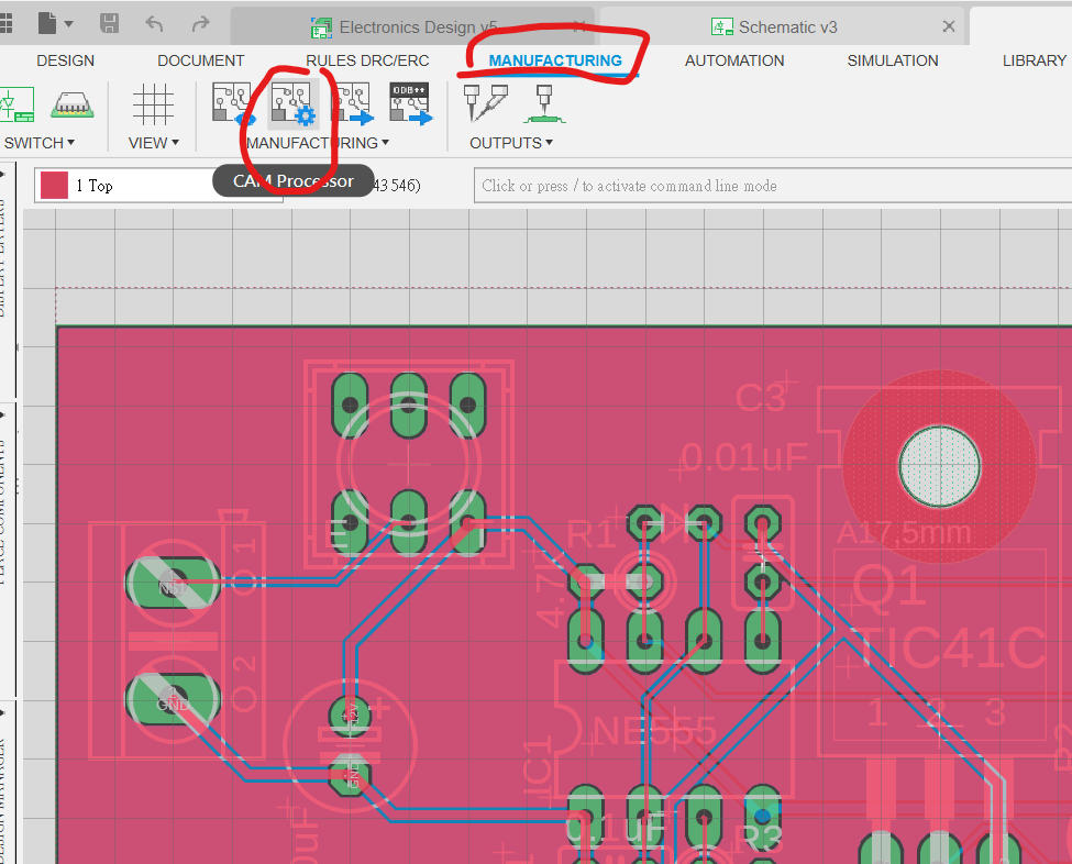
Open CAM Processor from the toolbar.
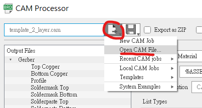
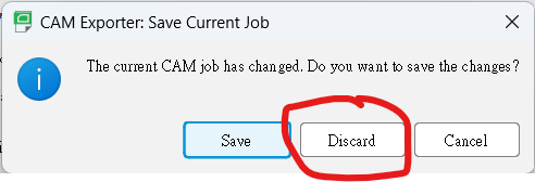
Choose Load Job File and then Open CAM File.
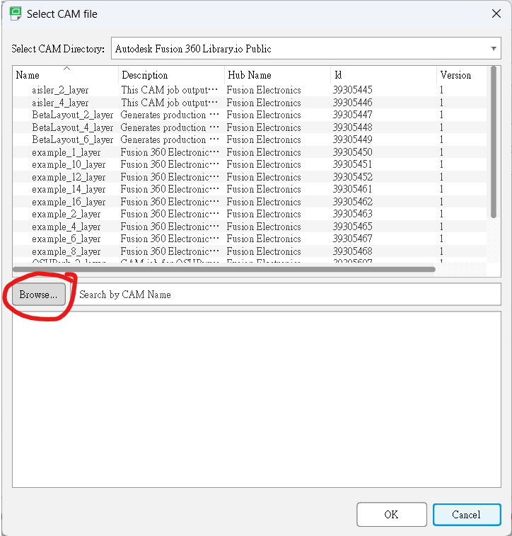
ℹ️INFO
Download the two-layer JLCPCB CAM job.
Locate and open the downloaded file.
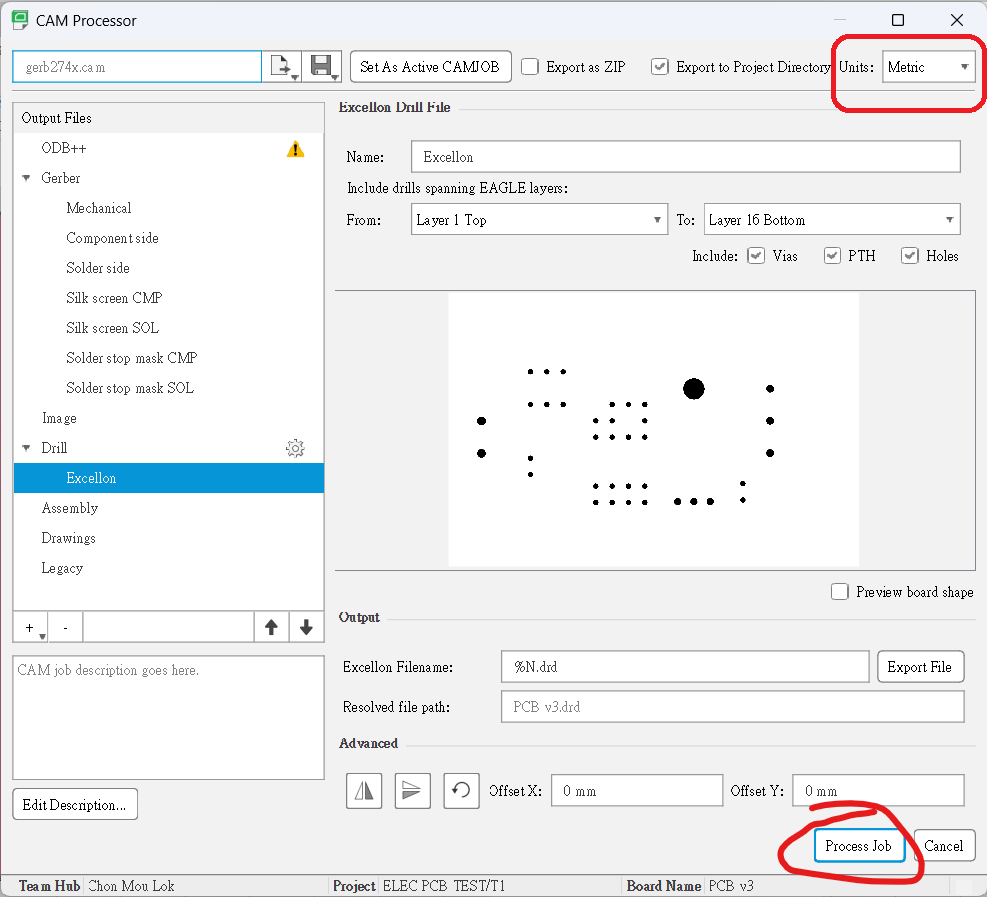
Confirm that the seven Gerber sections and the drill section are present, and that the unit is Metric. Click Process Job.
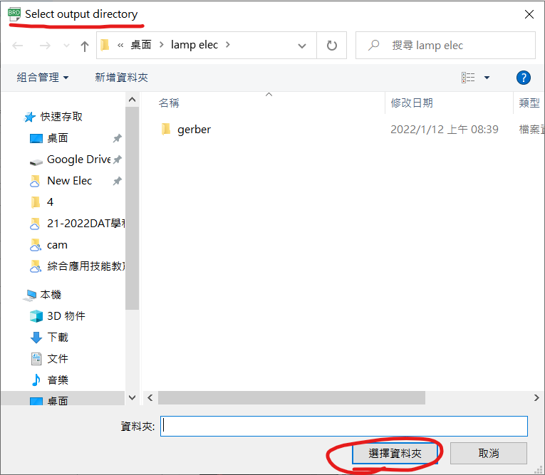
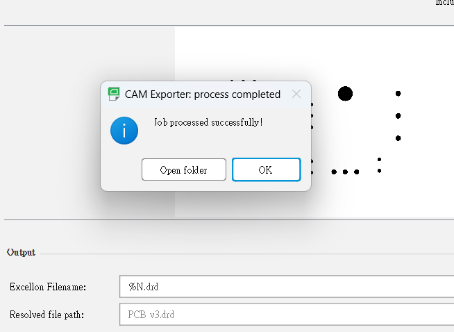
The output folder should contain the CMP, GKO, PLC, PLS, SOL, STC, STS and DRD files.
Upload the Manufacturing Files
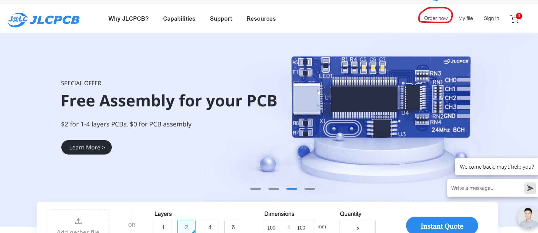
Visit JLCPCB and choose Order Now.
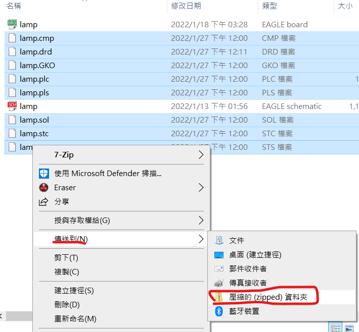
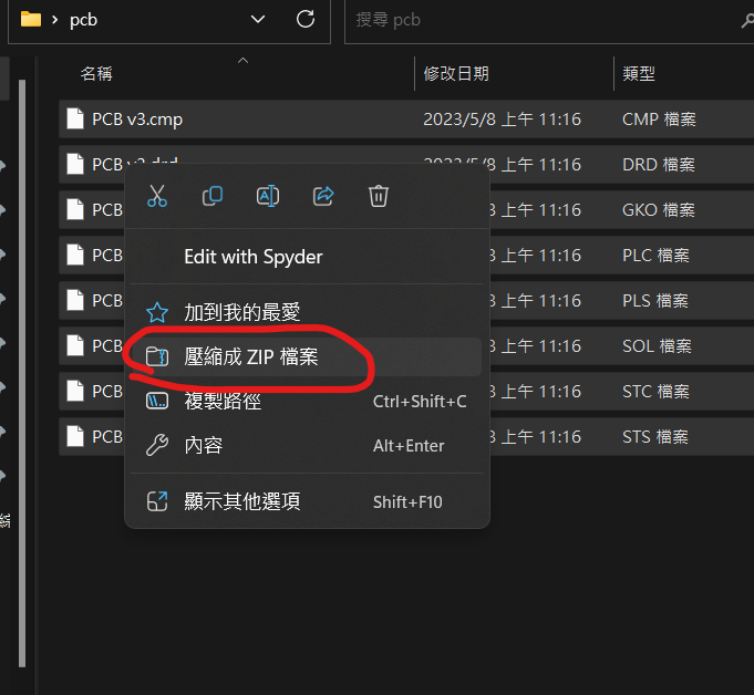
Select all eight manufacturing files and compress them into one ZIP archive.
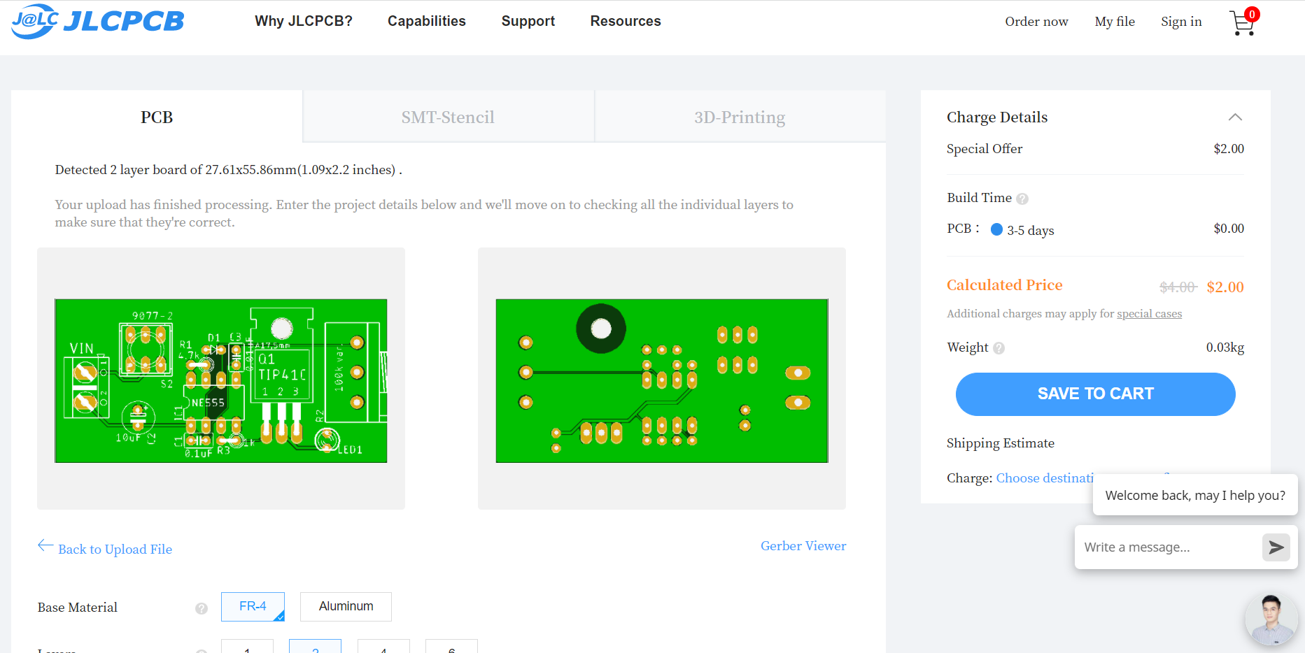
Drag the ZIP file onto the order page. The service should detect a two-layer board and show a preview. Inspect the silkscreen carefully for text that is too small or overlapping. Copper-rule errors should already have been caught by DRC.
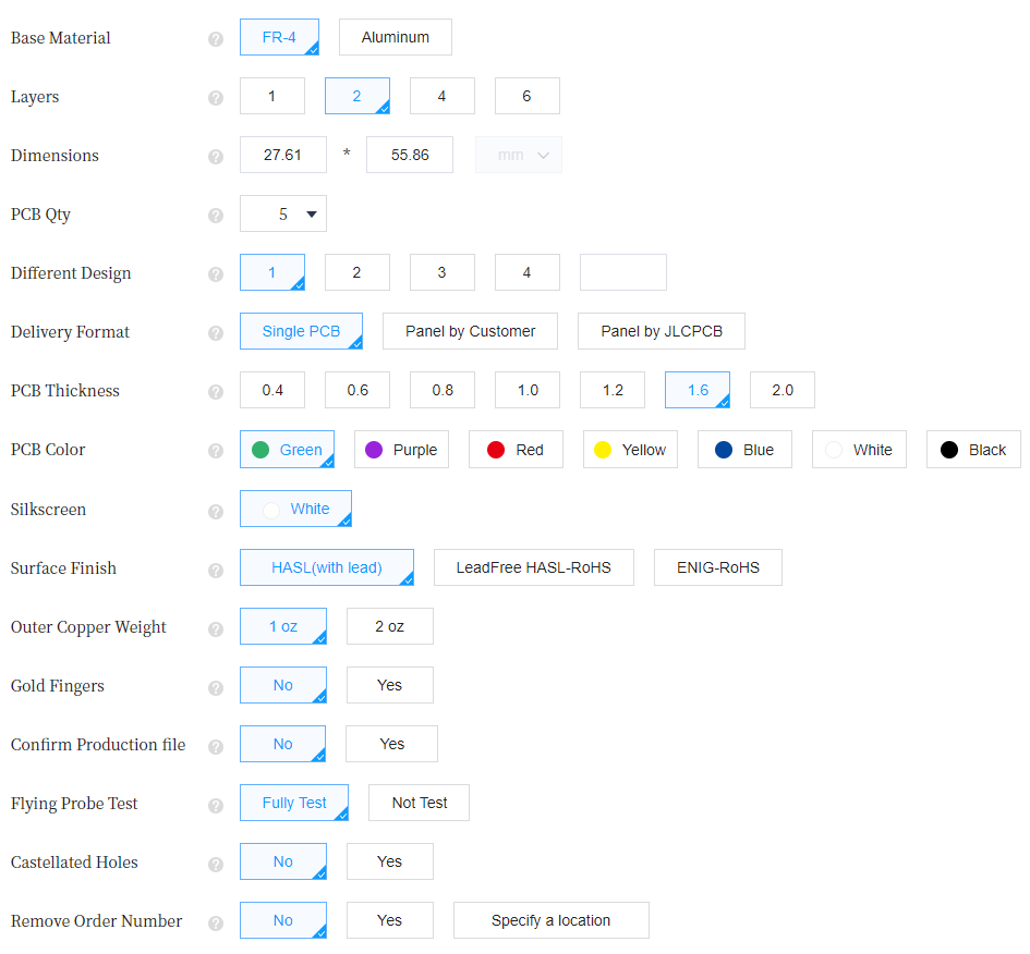
Review the main parameters:
Base Material: normally FR-4 glass-fibre laminate. Aluminium is often used for LED boards that need better heat dissipation.
Layers: choose 2 for this design.
Dimensions: detected automatically from the Gerber outline.
PCB Qty: the number of boards. The minimum is commonly five; price does not rise linearly with quantity.
Different Design: the number of different designs combined in one panel/order.
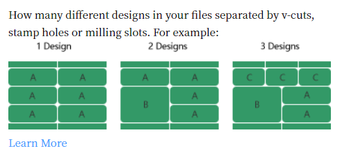
Delivery Format:
Single PCBseparates every board. Panel options leave multiple boards connected like postage stamps.PCB Thickness:
1.6 mmis common. Other thicknesses may affect cost and lead time.PCB Color: solder-mask colour. Some colours cost more or take longer.
Silkscreen: normally white, or black on a white solder mask.
Surface Finish: protects exposed copper pads from oxidation and improves solderability. Basic boards commonly use HASL; more expensive finishes include ENIG.
Outer Copper Weight: normally
1 oz. Consider2 ozonly for higher-current designs; it costs more and may take longer.Gold Fingers: used on plated edge contacts such as computer RAM connectors.
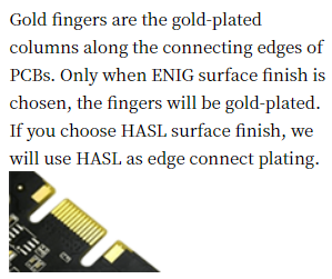
Confirm Production File: asks you to approve factory production artwork. Usually leave this off unless manual confirmation is required.
Flying Probe Test: electrically checks finished boards for open and short circuits;
Fully Testis normally appropriate.Castellated Holes: plated half-holes used when one PCB is soldered onto another as a module.
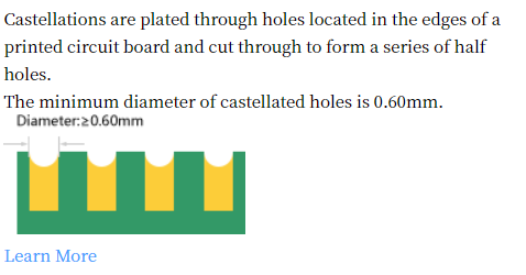
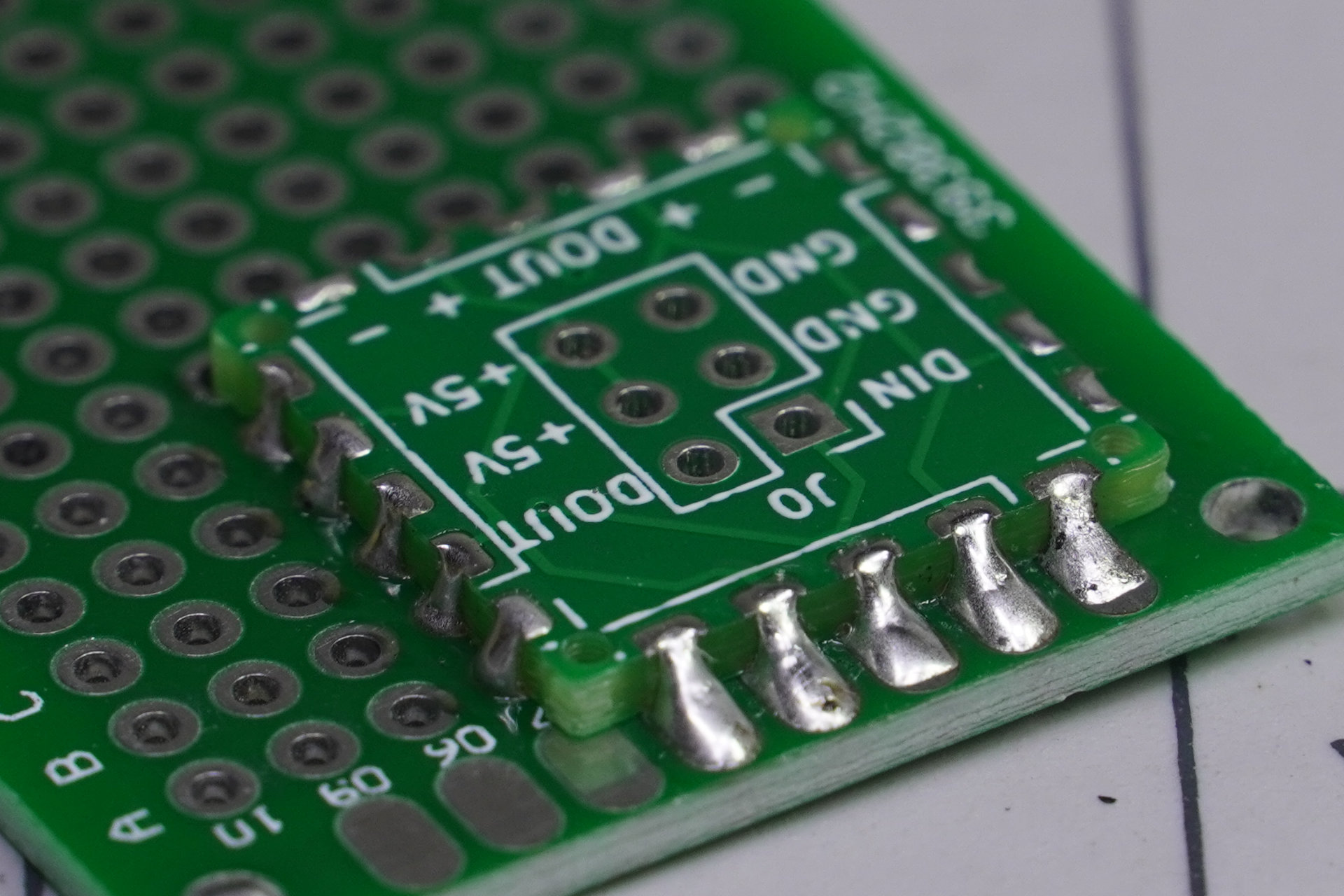
Remove Order Number: factories usually print a small tracking number on each order. You can pay to remove it or specify its location, but retaining it reduces the risk of factory mix-ups.
Other Services
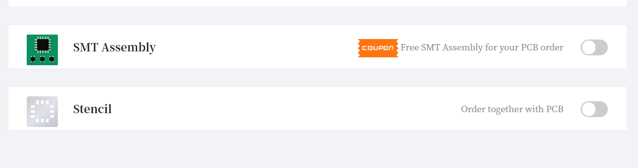
PCB manufacturers commonly offer two additional services:
- SMT Assembly: the factory solders surface-mount parts. There is usually a setup charge plus a per-part fee. Check stock availability and any programming requirements, such as burning a bootloader into an Arduino microcontroller. Assembly also requires a BOM and placement/manufacturing files.
- Stencil: a laser-cut metal stencil for applying solder paste. It is useful when a board contains many SMD parts: align the stencil over the pads, spread paste across it, place the parts, then reflow with hot air or a hot plate.
Translation notice: This English page was generated automatically by AI and has not yet been reviewed by a human. It will be checked and revised page by page when time permits.