Printed Circuit Boards (PCB)
ℹ️INFO
A printed circuit board, usually abbreviated PCB (or sometimes PWB), mechanically supports electronic components and connects them with metal conductors. Traditional boards were made by printing an etch-resistant pattern, which gave the technology its name. Modern fine-pitch boards more commonly use laminated or coated photoresist, exposure and development before the unwanted copper is etched away.
Introduction
A PCB consists mainly of an insulating substrate and conductive metal layers. Common boards contain 1, 2, 4 or 6 copper layers.
Single-Sided Board
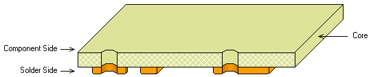
A single-sided PCB has a substrate and one copper routing layer. The substrate is usually FR-4 glass-fibre laminate, although aluminium-core boards may be used to improve heat dissipation.
Double-Sided Board
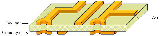
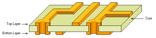
A double-sided board has copper tracks on both sides of the substrate. The circuits on the front and back usually need to connect, so copper plating is added inside selected holes to create electrical connections between the two sides.
Solder Mask
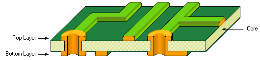
The coloured coating—commonly green—protects and insulates the finished circuit. Openings in this solder mask expose copper so that components can be soldered. Copper may also be intentionally exposed so that solder can be added to increase the current-carrying capacity of a track.
Via
A via is a deliberately drilled and copper-plated hole that electrically connects tracks on different copper layers.
Silkscreen Layers
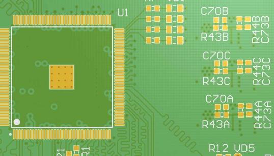
The silkscreen is the printed text and markings on a board. It helps the assembler identify and position components correctly.
PCB Manufacturing Process
- Begin with copper-clad laminate. Copper weight is commonly specified as 1 oz/ft² or 2 oz/ft². A 2 oz board is substantially more expensive, so 1 oz is normally sufficient.
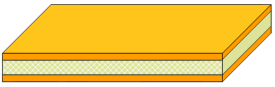
- A CNC machine drills the PCB.
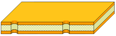
- Both sides are covered with photosensitive etch resist.
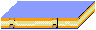
- A negative artwork masks the areas to be etched and leaves the circuit pattern exposed to UV light of the required wavelength.
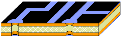
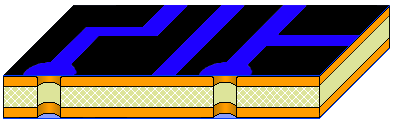
- Exposure hardens the illuminated resist. The unhardened resist is then developed and washed away.
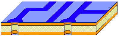
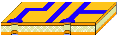
- The board is immersed in an etchant that removes unwanted copper, leaving the circuit pattern. The remaining hardened resist is then cleaned away.
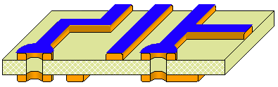
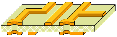
- The board is plated so that the walls of vias and other drilled holes are coated with copper.
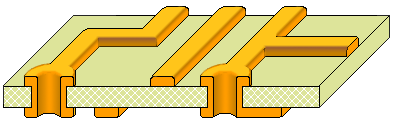
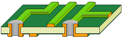
- Similar photographic processes apply the solder mask and white silkscreen. Finally, exposed copper is finished with tin or, in some processes, gold.
Surface-Mount and Through-Hole Technology (SMD and THT)
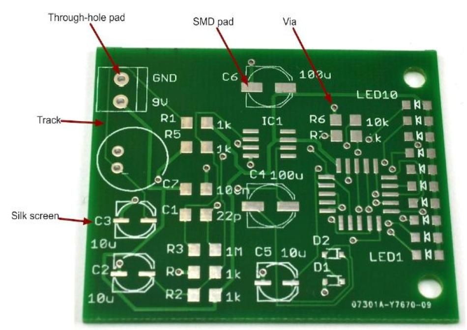
The photograph identifies the features introduced above. White reference text belongs to the silkscreen; copper conductors are called tracks; and the board also contains through-hole pads, SMD pads and vias.
Through-Hole vs Surface-Mount Components
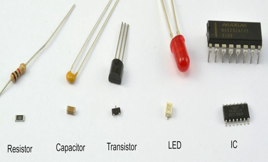
Consumer electronics from the 1980s and 1990s often used mostly through-hole components. Manufacturing was less advanced, circuits were generally less dense, and through-hole parts were easier to solder by hand. Since the 2000s, circuits have become more complex and multilayer boards increasingly common, so most mass-produced electronics use surface-mount devices. SMD parts are much smaller and their leads do not pass through the board, leaving inner and opposite-side layers free for denser routing. Many modern integrated circuits are now released only in SMD packages rather than THT versions.
Source: Altium
Translation notice: This English page was generated automatically by AI and has not yet been reviewed by a human. It will be checked and revised page by page when time permits.