Making a PCB at Home
This chapter uses a 555 + 4017 LED chaser to demonstrate toner-transfer PCB fabrication.
Draw the Schematic
Create the schematic by following Drawing Schematics and PCB Layouts.
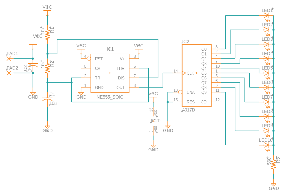
| Part | Value | Device | Package | Library |
|---|---|---|---|---|
| C1–C2 | 10u | C-USC0805K | C0805K | rcl (Version 11) |
| IC1 | NE555_SOIC | NE555_SOIC | SOIC127P599X175-8N | IC_Clock-Timing |
| IC2 | 4017D | 4017D | SO16 | 40xx (Version 7) |
| LED1–LED10 | LEDCHIP-LED0805 | CHIP-LED0805 | adafruit (Version 2) | |
| PAD1–PAD2 | SMD2 | SMD1,27-2,54 | wirepad (Version 2) | |
| R1–R2 | 10k | R-US_R0805 | R0805 | rcl (Version 11) |
| R5 | 560 | R-US_R0805 | R0805 | rcl (Version 11) |
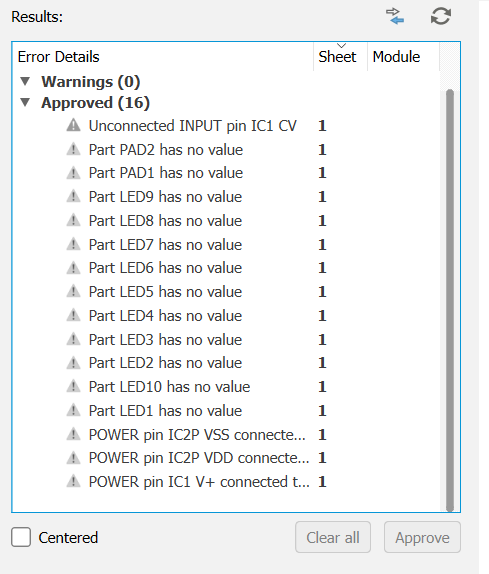
Run ERC when finished. Review the expected warnings and mark them Approved; correct any actual errors.
Create the Board Layout
Place the Components
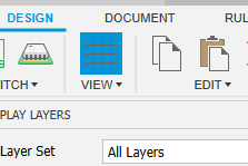
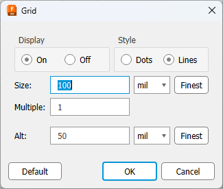
Set Grid to 100 mil and Alt to 50 mil.
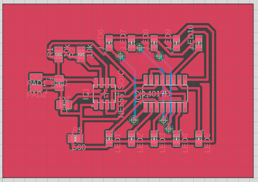
Arrange the parts approximately as shown. Follow the airwires and keep connected parts close together.
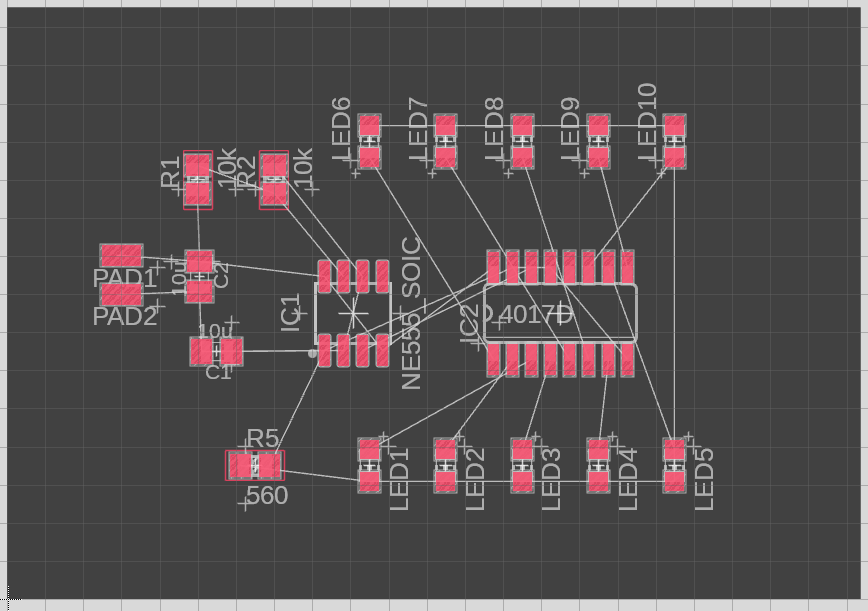
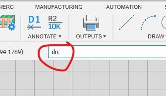
Factory defaults such as 6 mil tracks are too fine for reliable toner-transfer etching. Enter drc and enlarge the design rules.
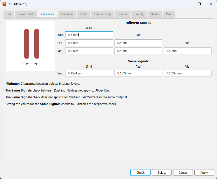
- Under
Clearance, set every Wire/Pad/Via spacing to0.5 mm. - Under
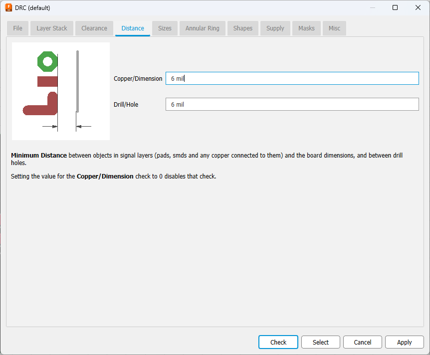
Distance, set Dimension to6 mil.
⚠️WARNING
Enter the mm unit explicitly where required.
- Under
Sizes, set Minimum Width to0.5 mmand Minimum Drill to0.9 mm. - Under
Masks, set Limit to3 mm.
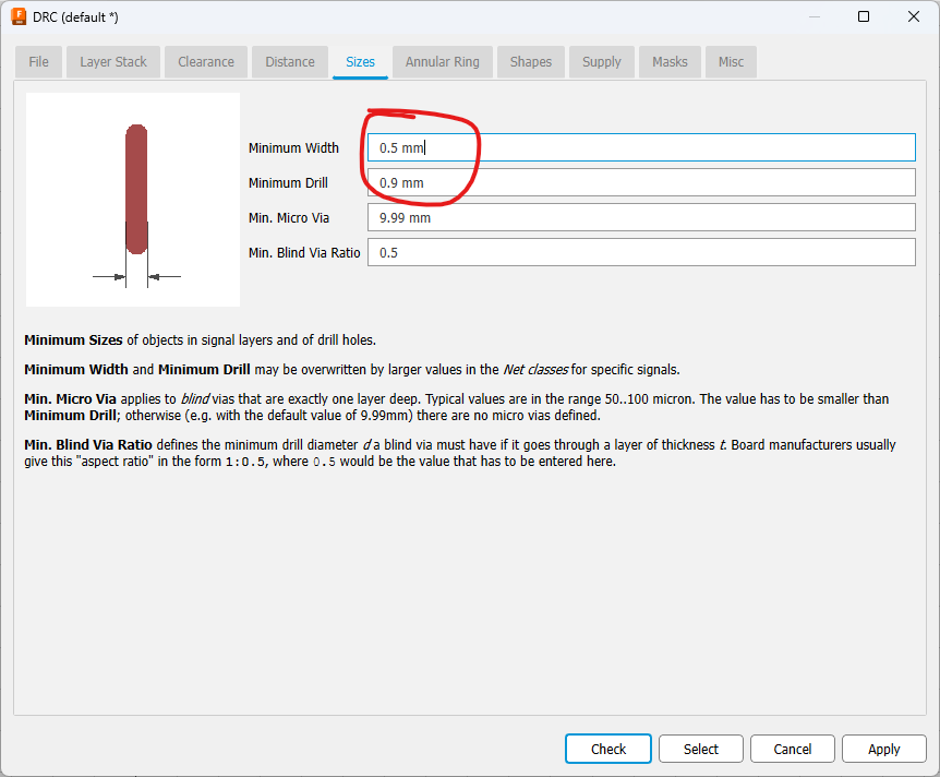
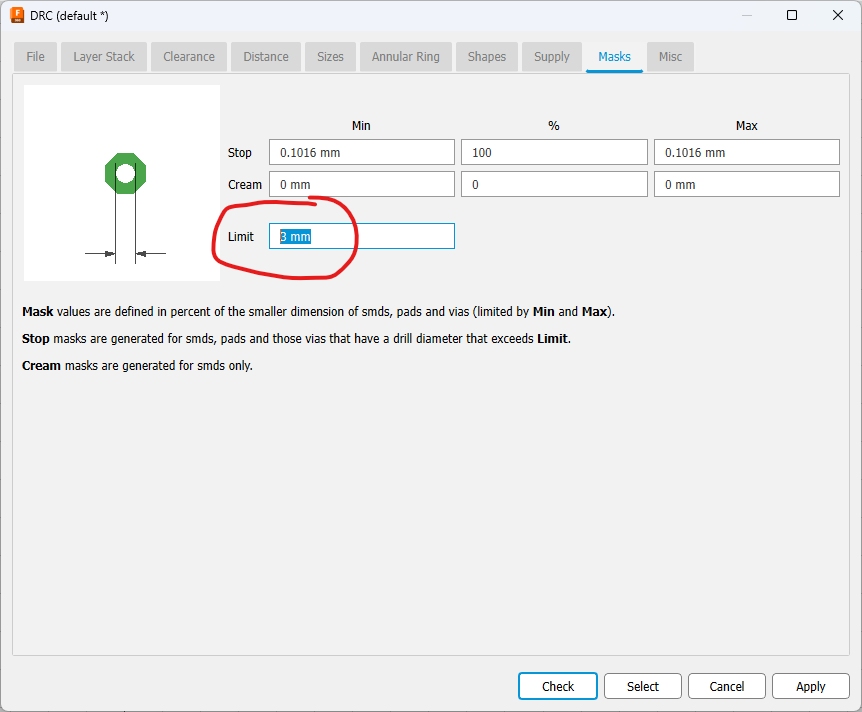
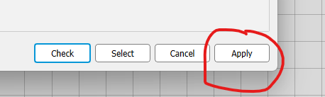
Click Apply, not Check.
Route the Board
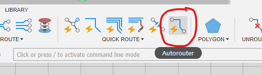
Start the autorouter.
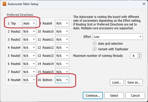
A home-made double-sided board would require many accurately drilled and plated/jumpered vias. For this exercise, route primarily as a single-sided board: leave 1 Top on Auto and set 16 Bottom to N/A.
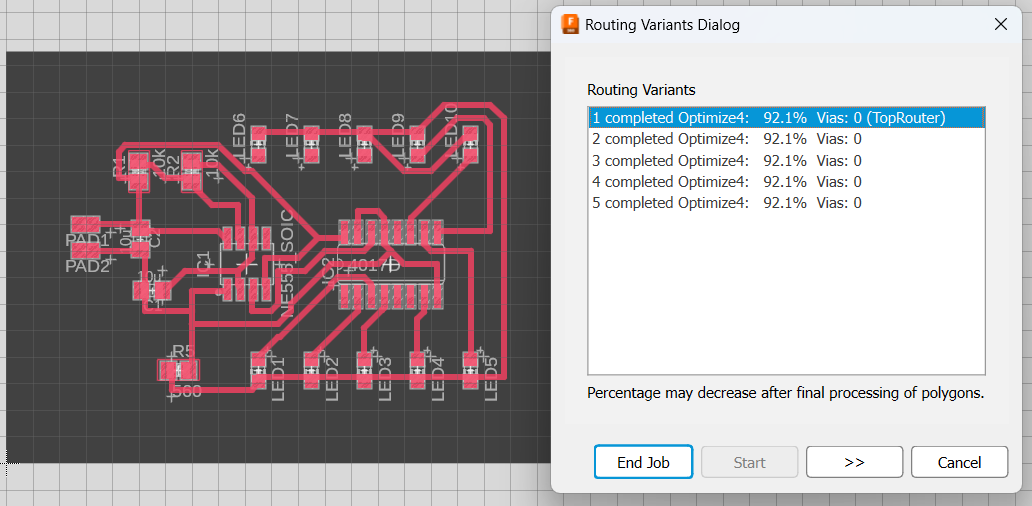
The autorouter may not reach 100%. If it remains below about 90%, enlarge the outline or improve placement. Choose a result with short routes and click End Job.
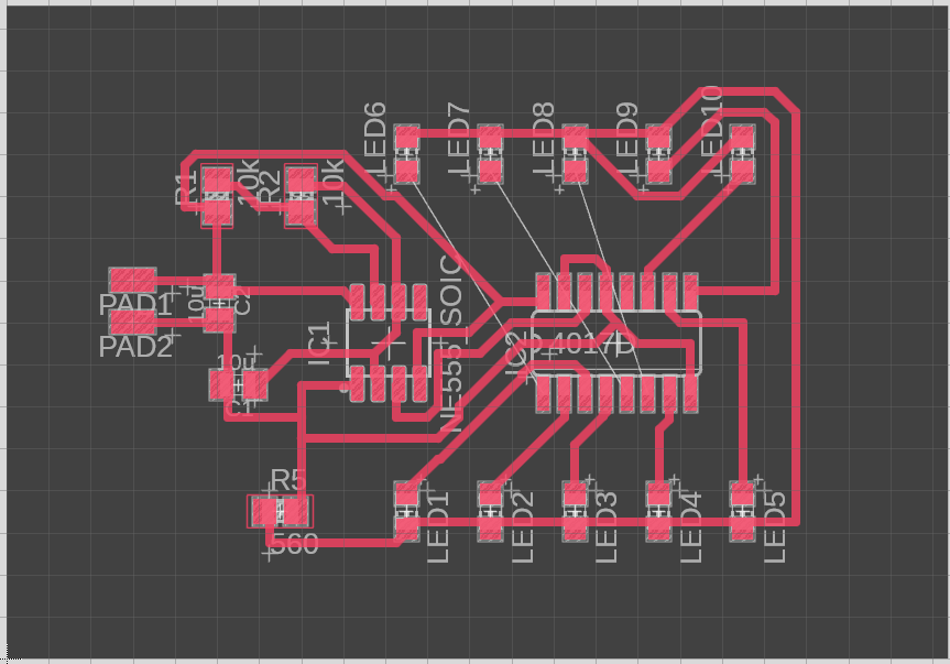
The example leaves three unrouted airwires.
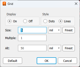
For manual routing, reduce Grid Size to 5 mil or less.
Choose Route and set width to 0.5 mm.
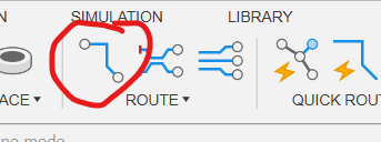
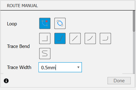
Click an unrouted airwire to begin a red top-layer track. Middle-click to place a via and continue on the blue bottom layer; middle-click again to place a second via and return to red. The example uses three short bottom-layer links and six vias.
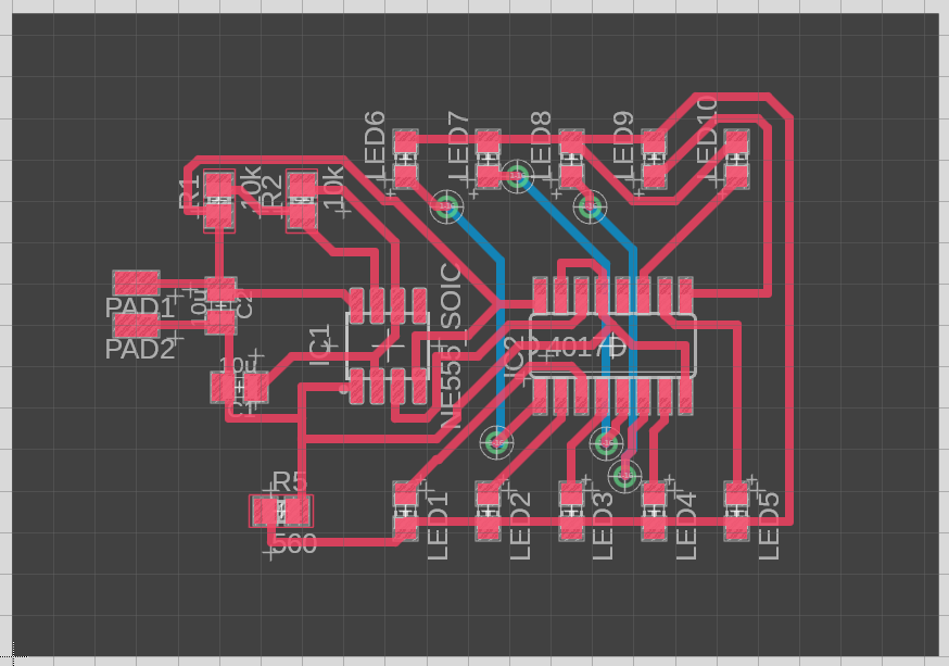
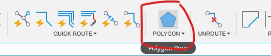
Draw a polygon around the outline. Retaining unused copper reduces etchant consumption and etching time.
Fabricate the Board
Print the Toner Artwork
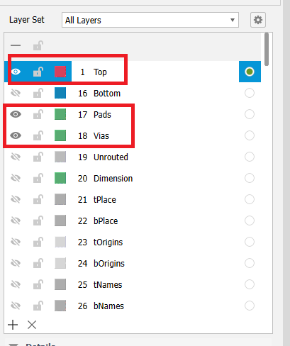
Under Display Layers, show only 1 Top, 17 Pads and 18 Vias.
Open Print.

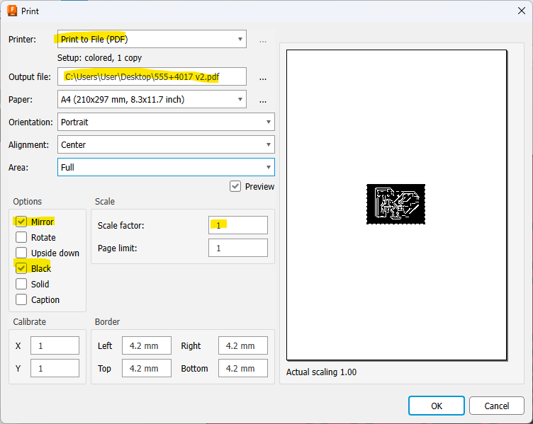
Choose Print to File (PDF), set an output path, enable Mirror and Black, and set Scale Factor to exactly 1 for full-size output.
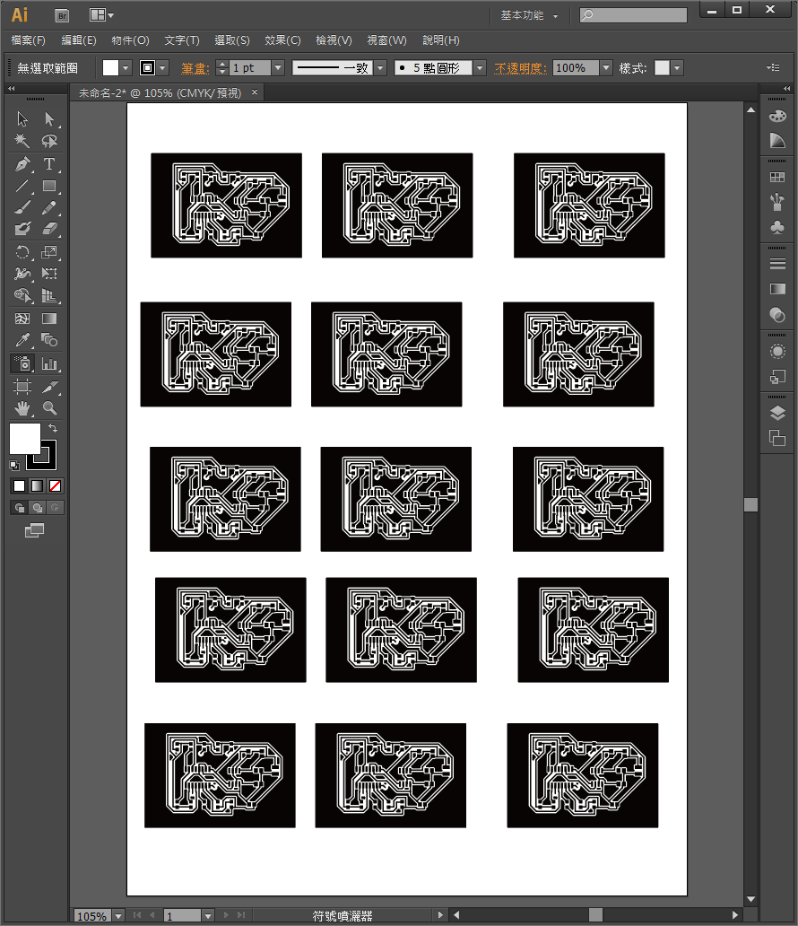
Lay out several copies in Illustrator, CorelDRAW or free Inkscape so that a failed transfer can be retried.
Print on the smooth side of toner-transfer paper with a laser printer. Inkjet printing will not work.
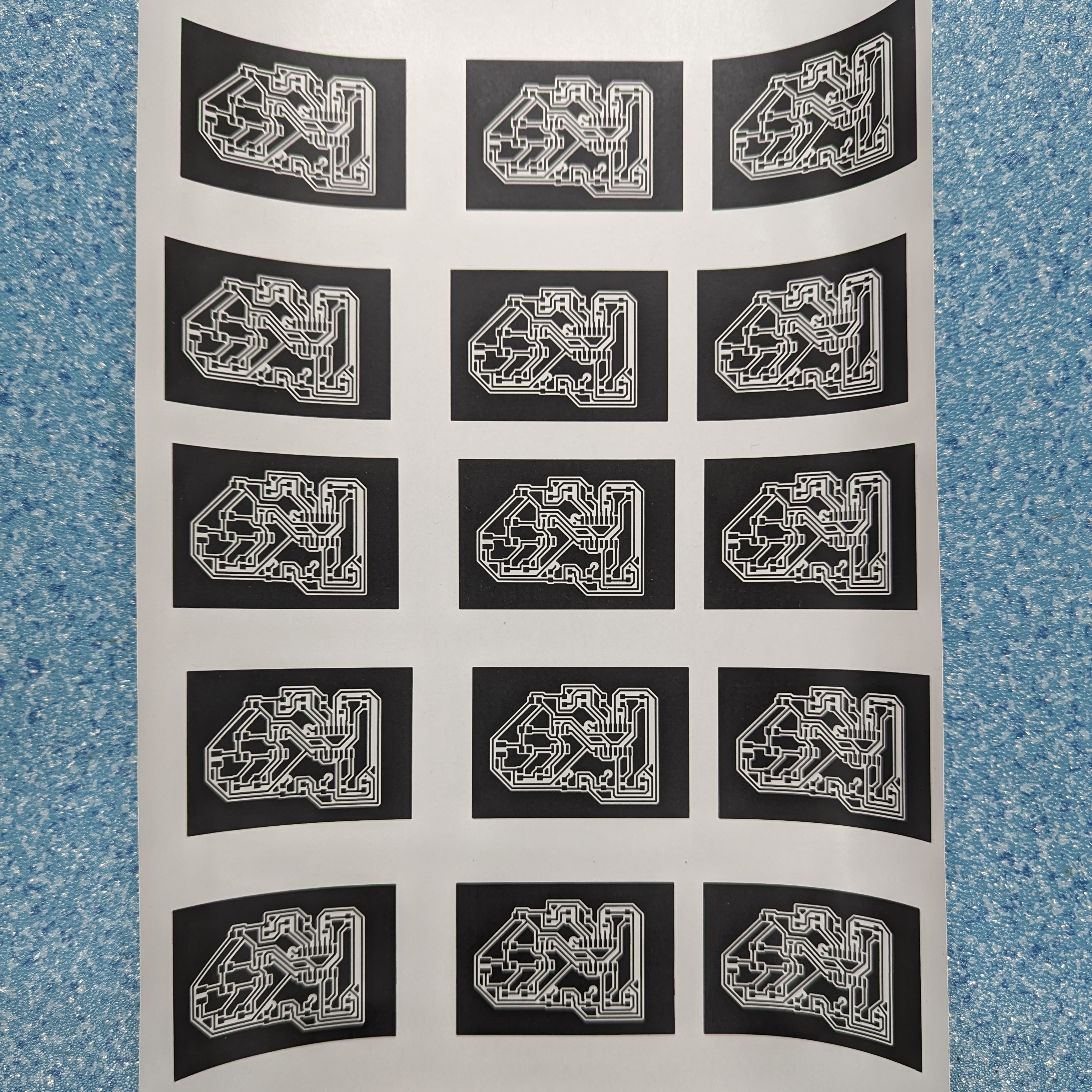
Prepare and Transfer
Cut copper-clad board to approximately 100 × 75 mm.
⚠️WARNING
Do not make it narrower than the transfer machine can grip; for the demonstrated machine, an edge below about 70 mm will not feed reliably.
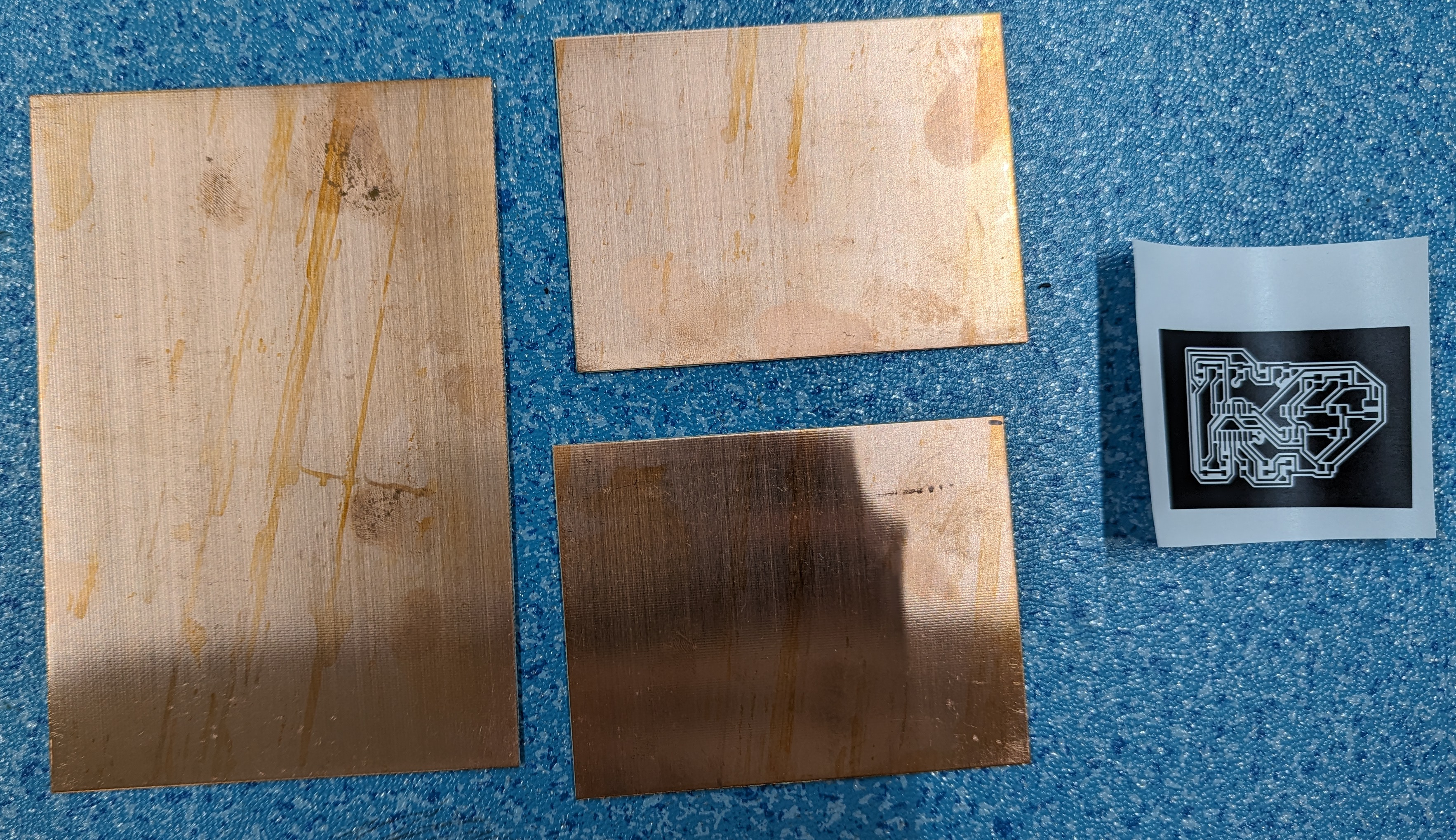
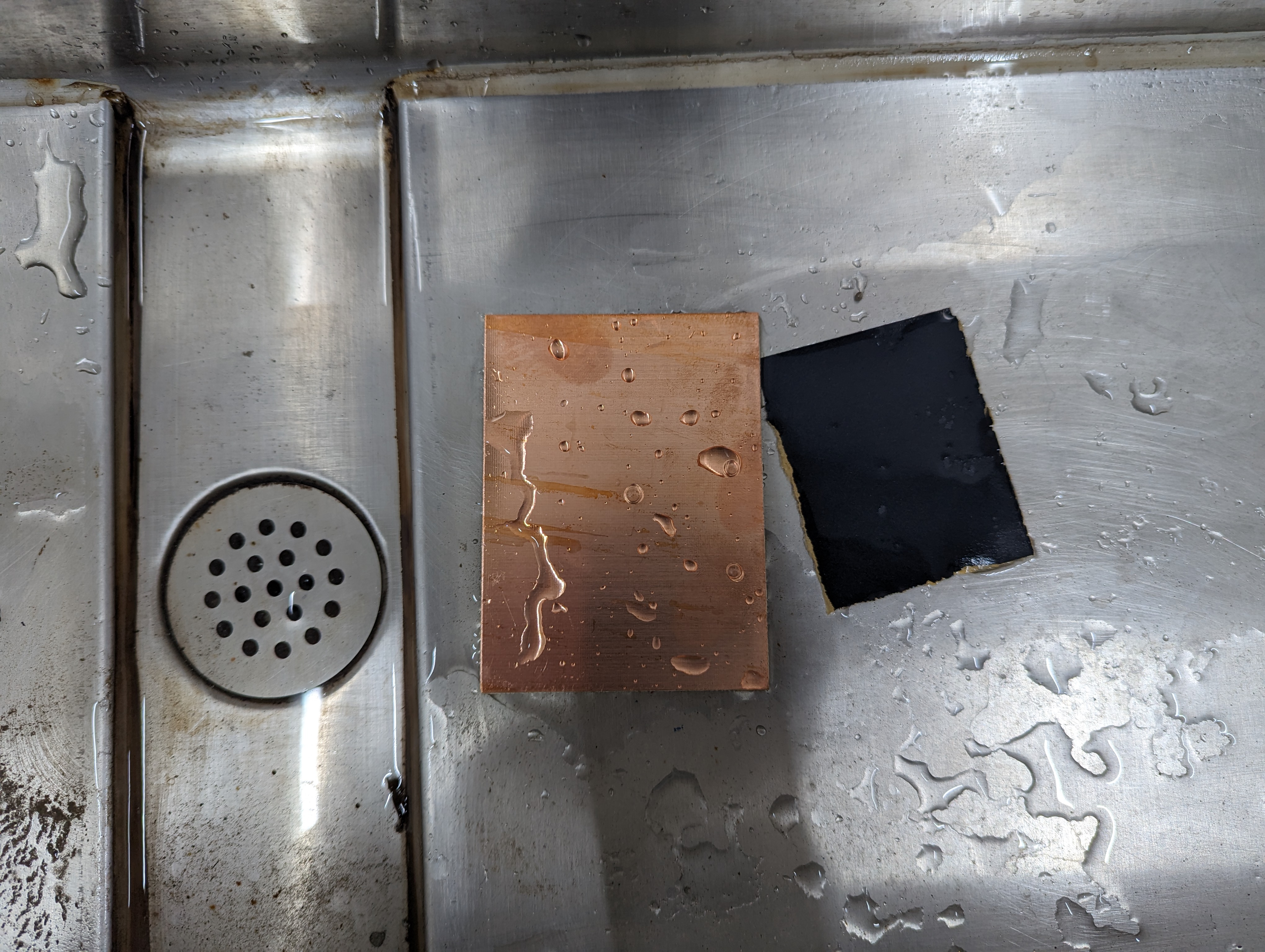
Wet-sand gently with 400-grit paper to remove oxide. Typical copper is only about 0.035 mm thick, so do not sand aggressively. Degrease both sides with detergent or an appropriate cleaner while wearing the required protection.
Dry with paper without touching the clean copper. Leave a 1–2 cm white margin when trimming the transfer artwork.
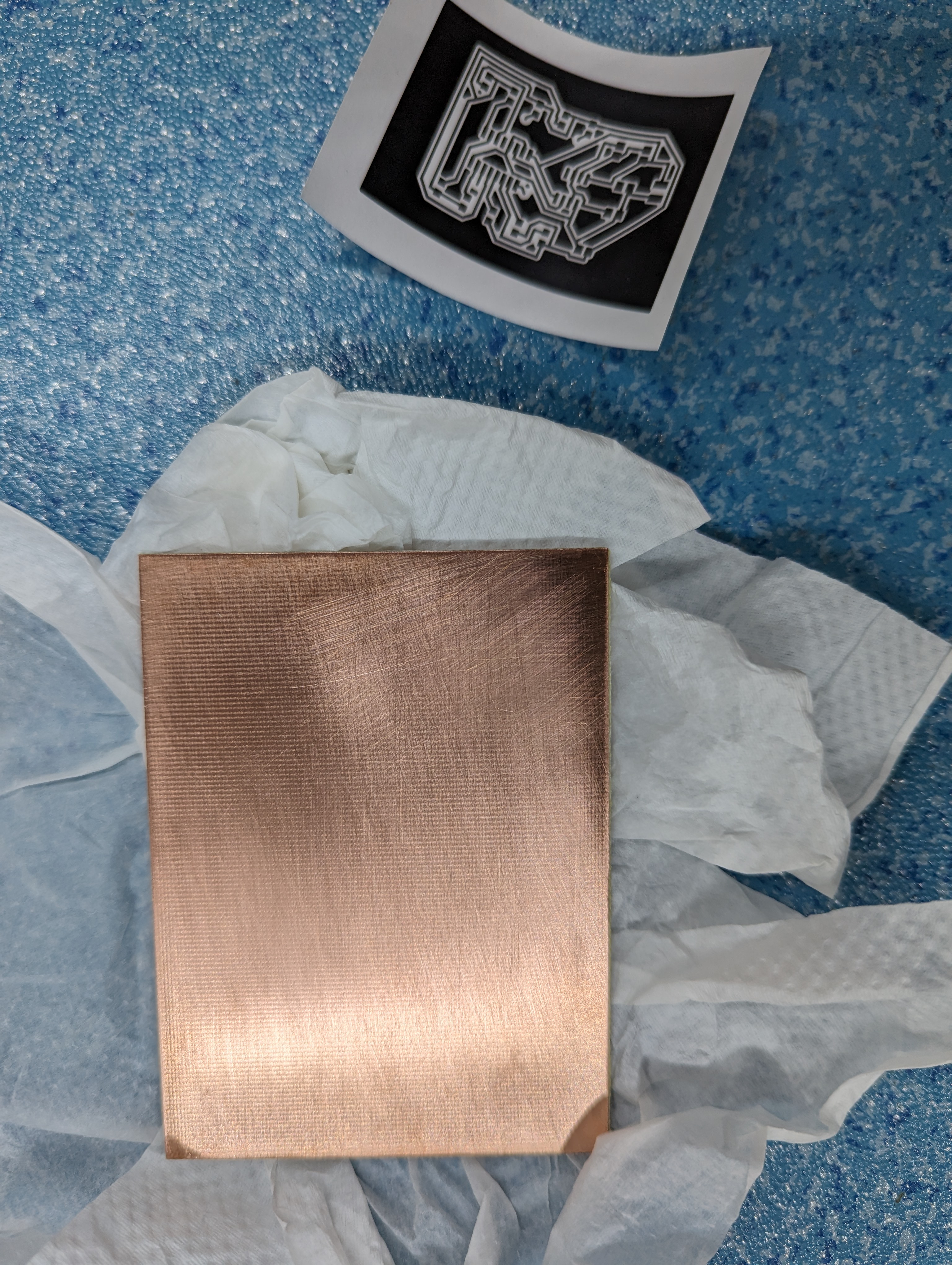
Attach it with heat-resistant tape. Do not cover any black toner. Centre the artwork, keep enough tape contact area, tape only one short edge and a small part of the long edges, and make sure the paper lies completely flat.
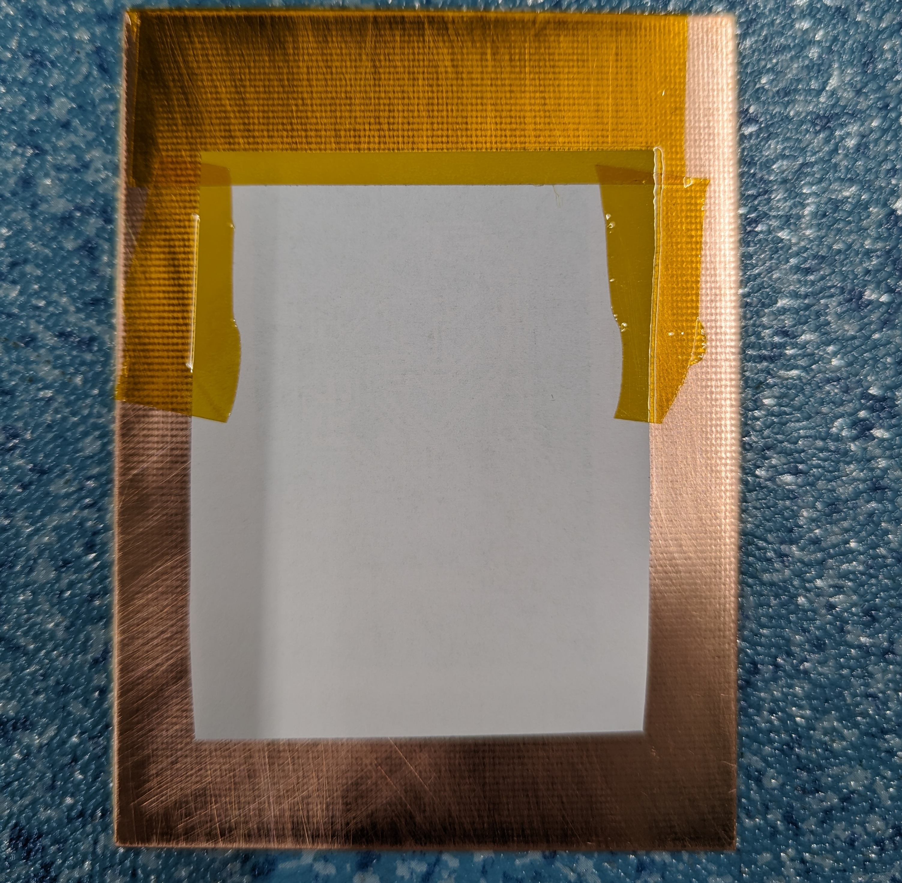
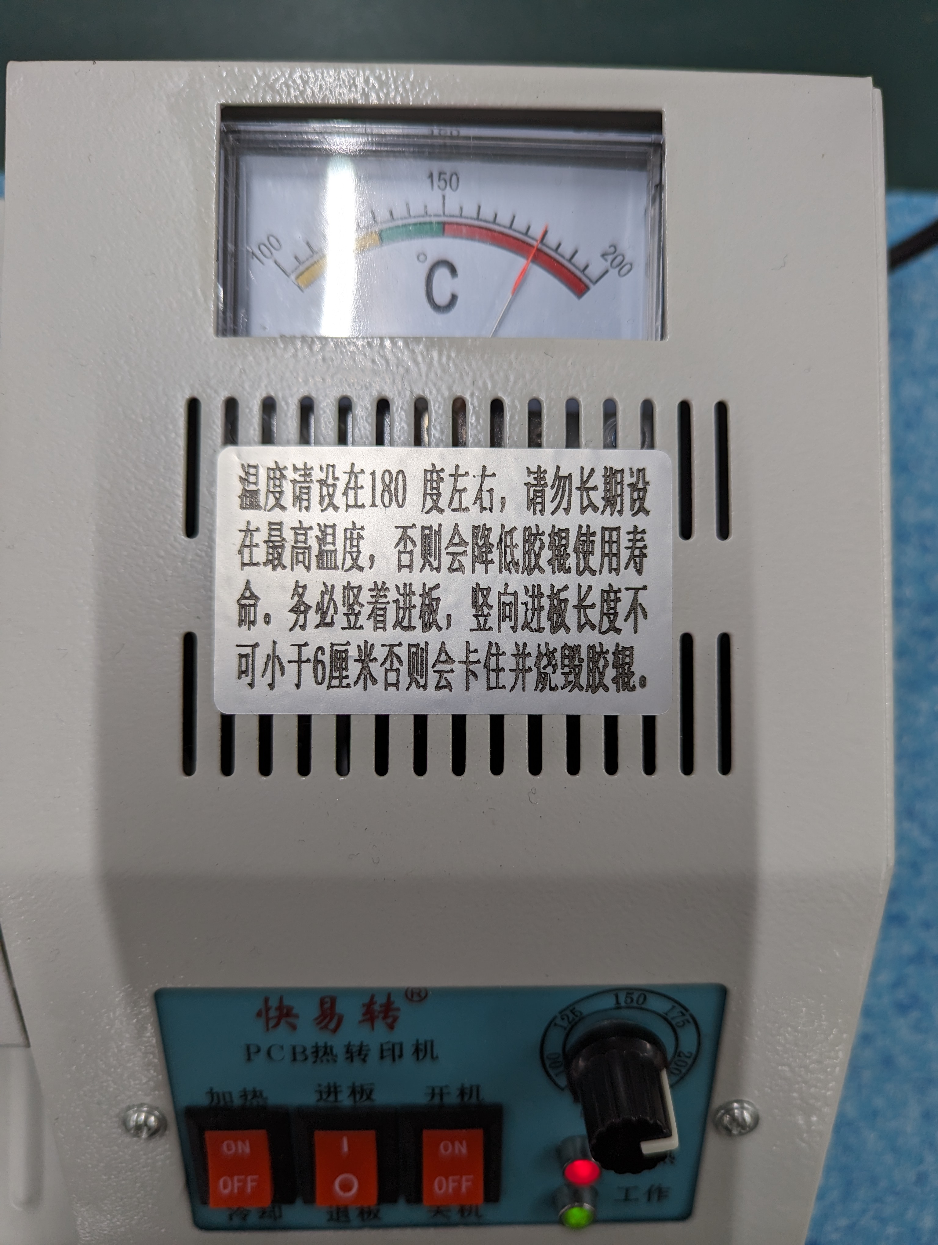
Set the demonstrated transfer machine to approximately 180°C. Feed the taped edge first and support the rigid board through the rollers. Pass it through twice.
⛔️DANGER
The board and rollers are extremely hot. Use suitable tools and heat protection; never touch the hot copper directly.
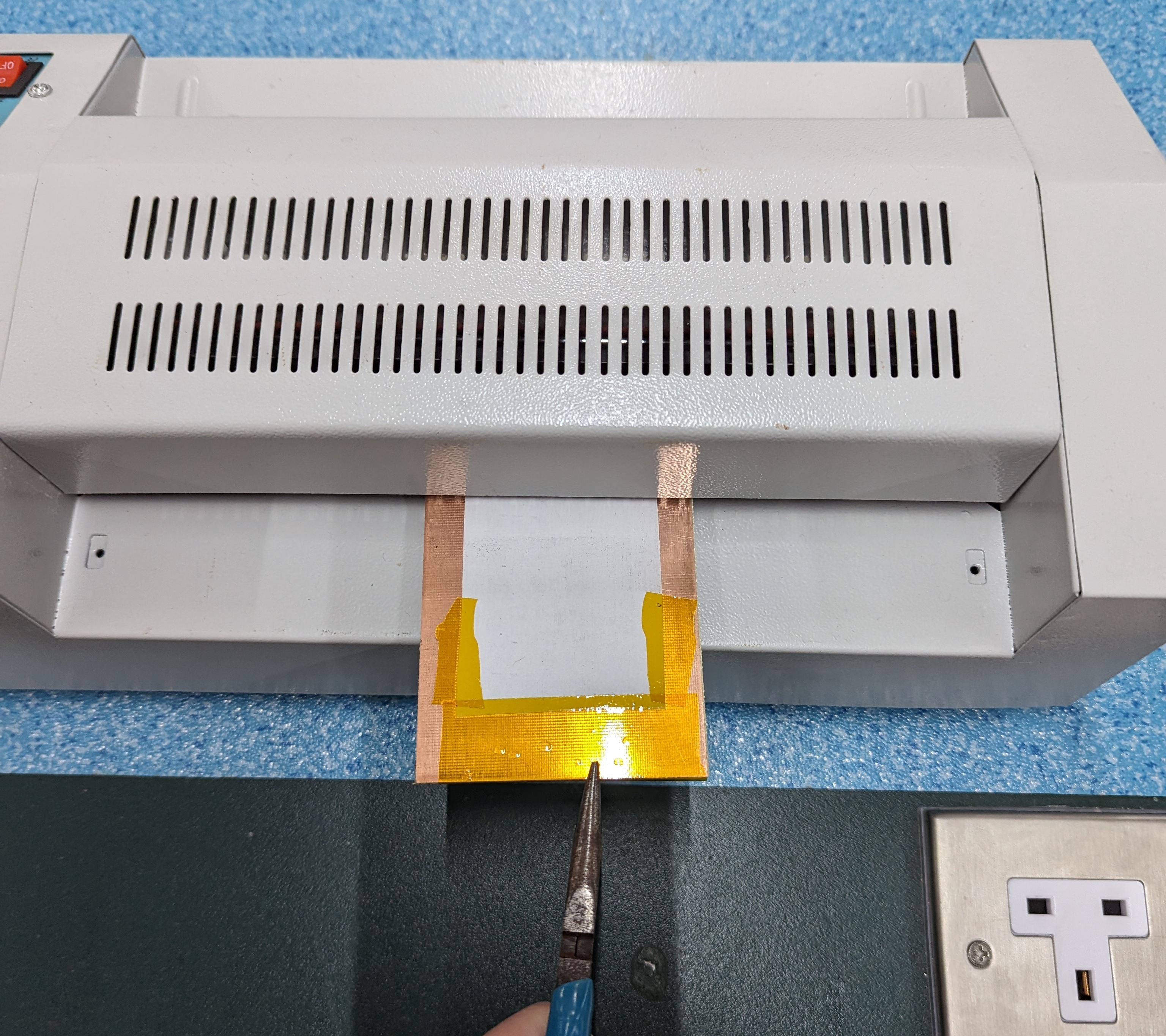
Let the board cool, then peel away the tape and transfer paper.
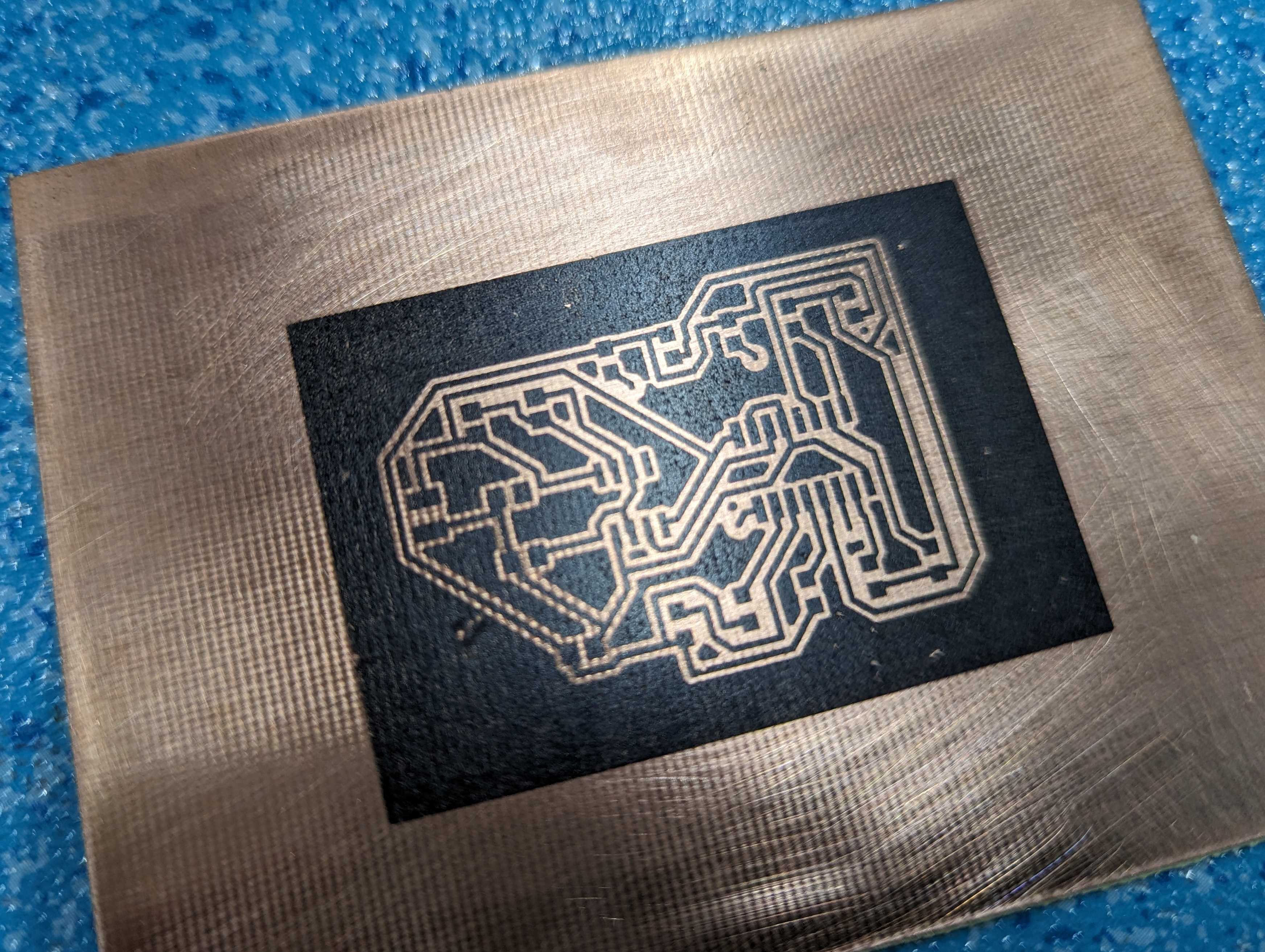
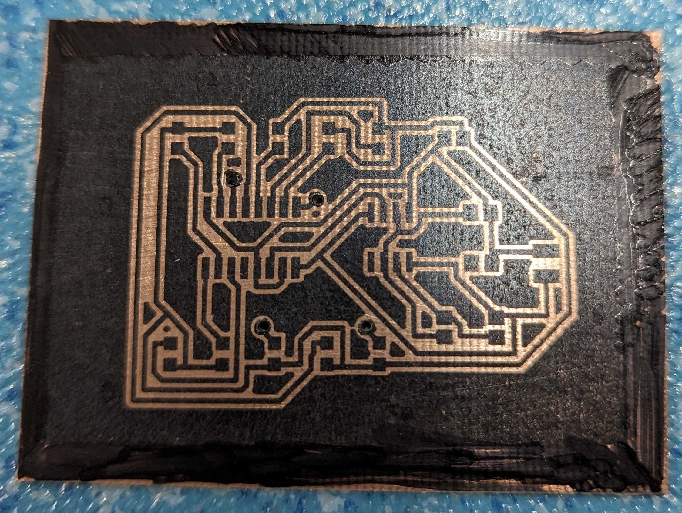
Inspect every track under magnification. Repair incomplete toner with a permanent marker, taking care around the 0.5 mm tracks and gaps.
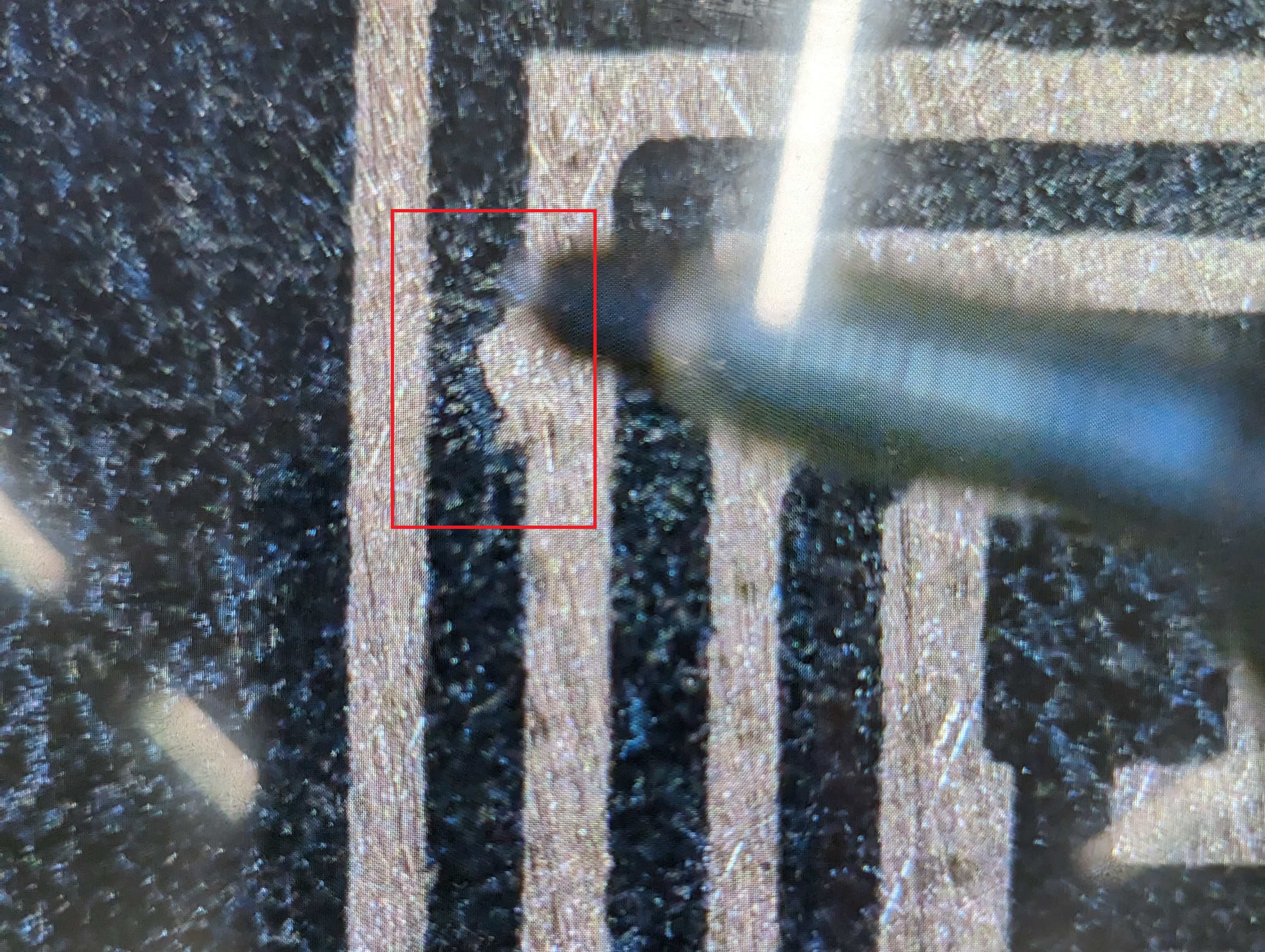
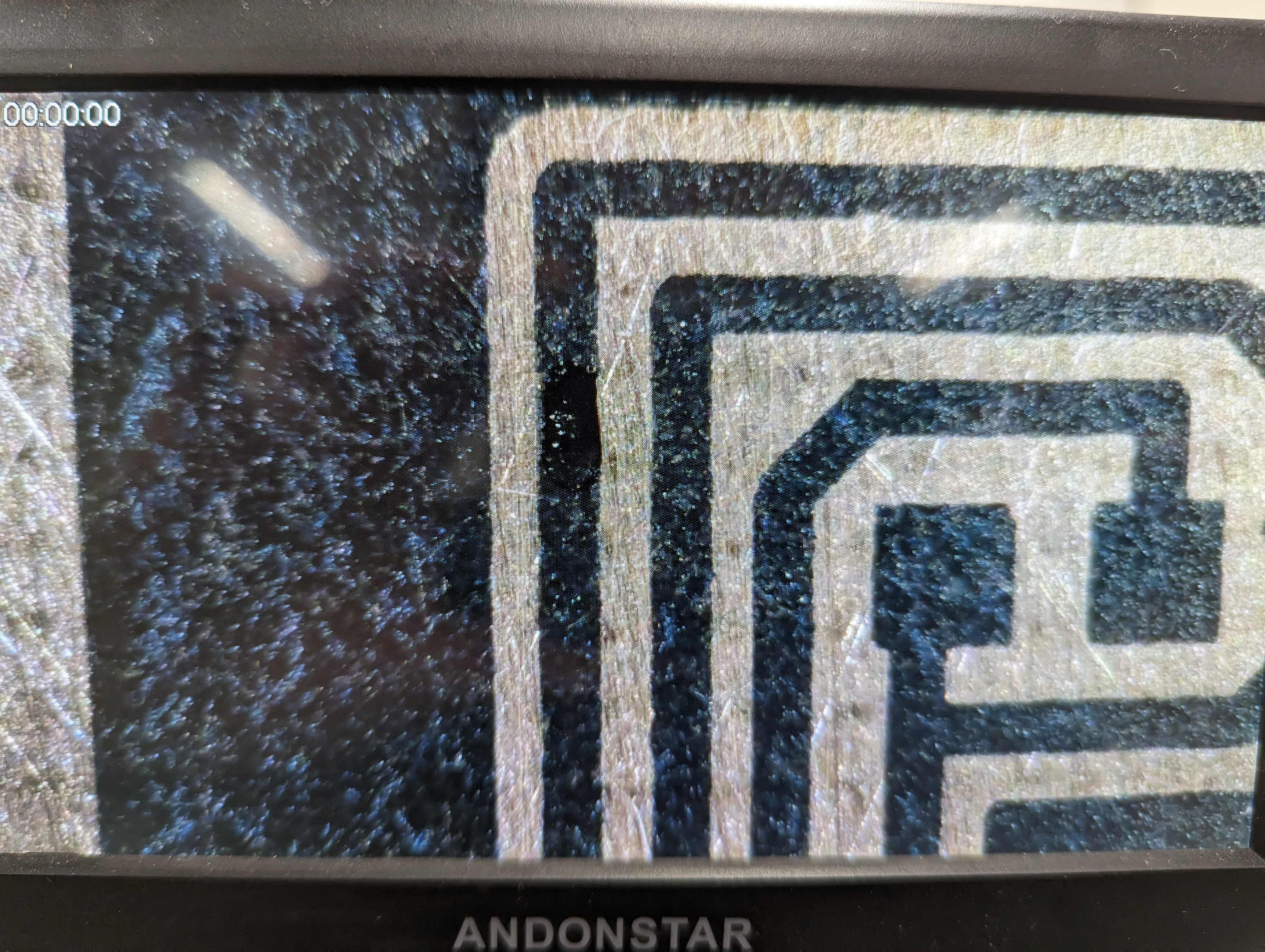
Protect the toner with A4 paper while trimming the board, leaving a 5–10 mm margin. Drill the 0.9 mm vias carefully and repair toner around their edges.
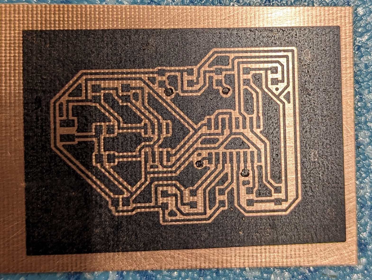
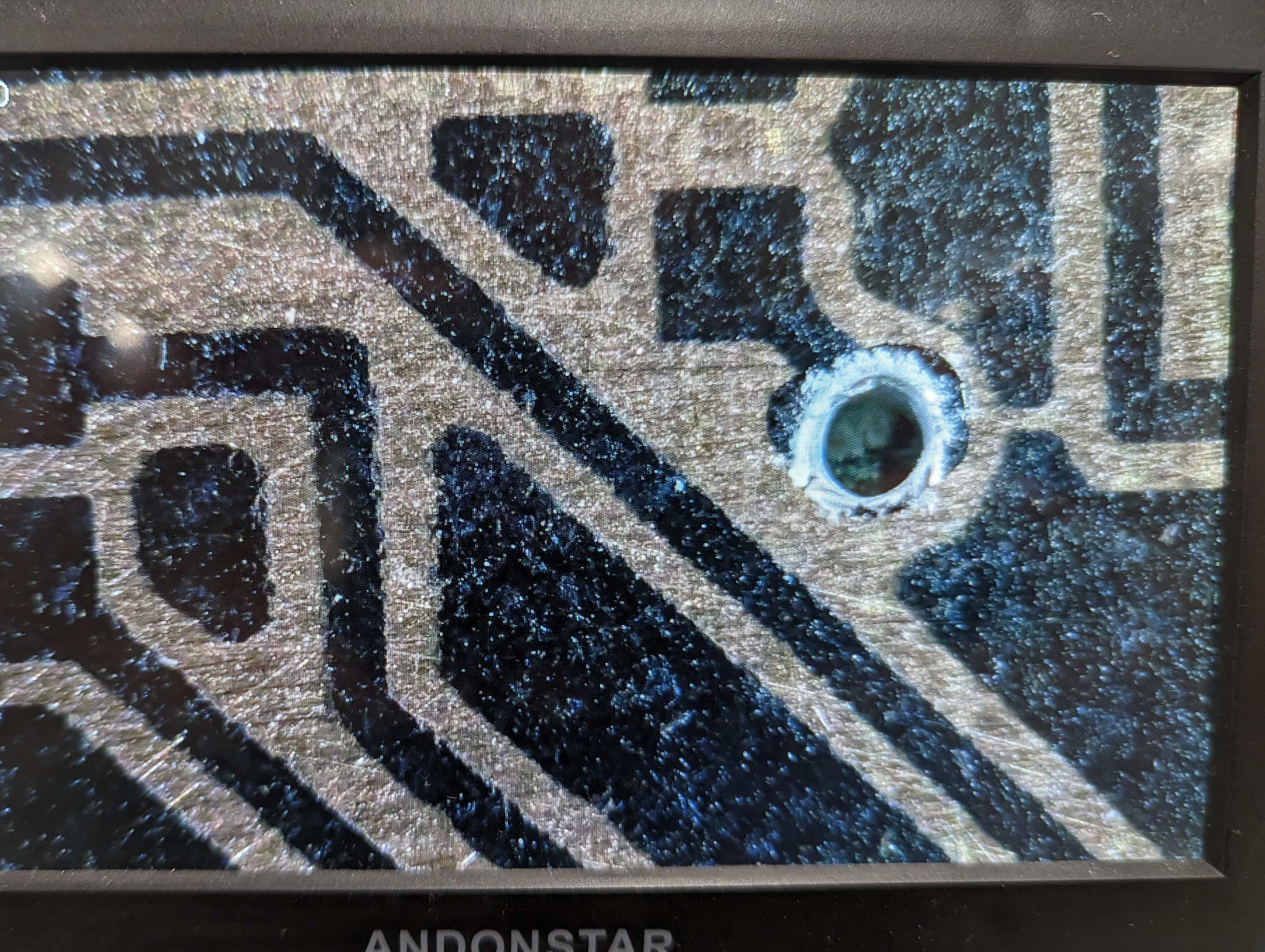
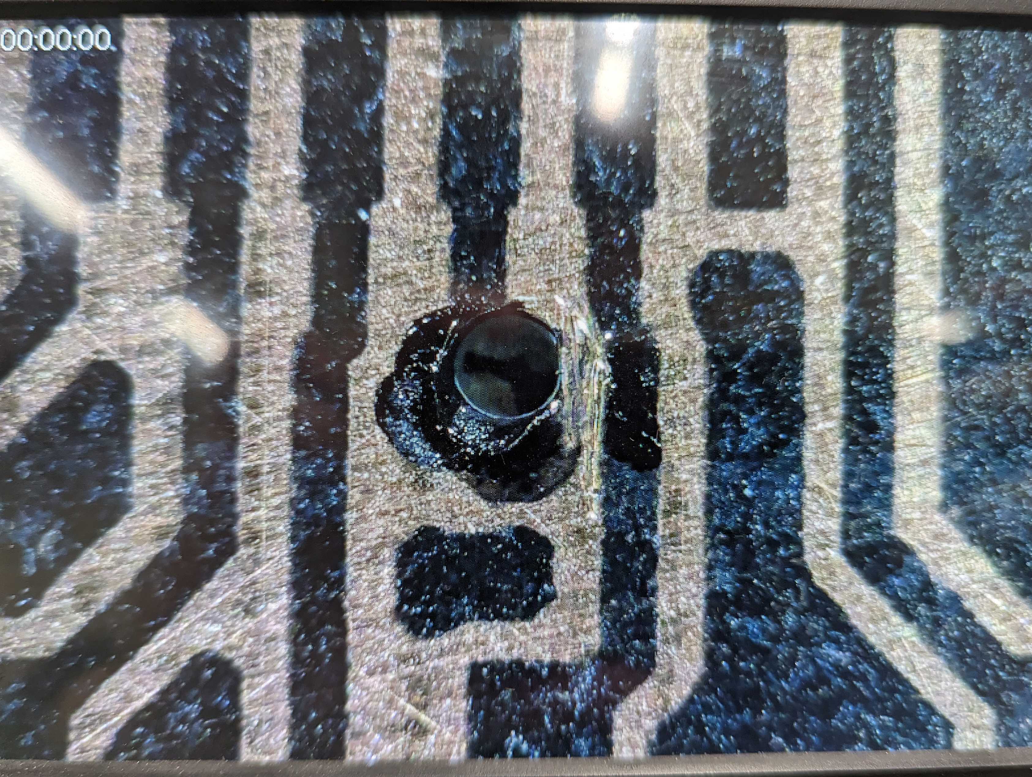
Cover all other copper that must remain. On the reverse, retain small copper links where useful instead of adding wire later.
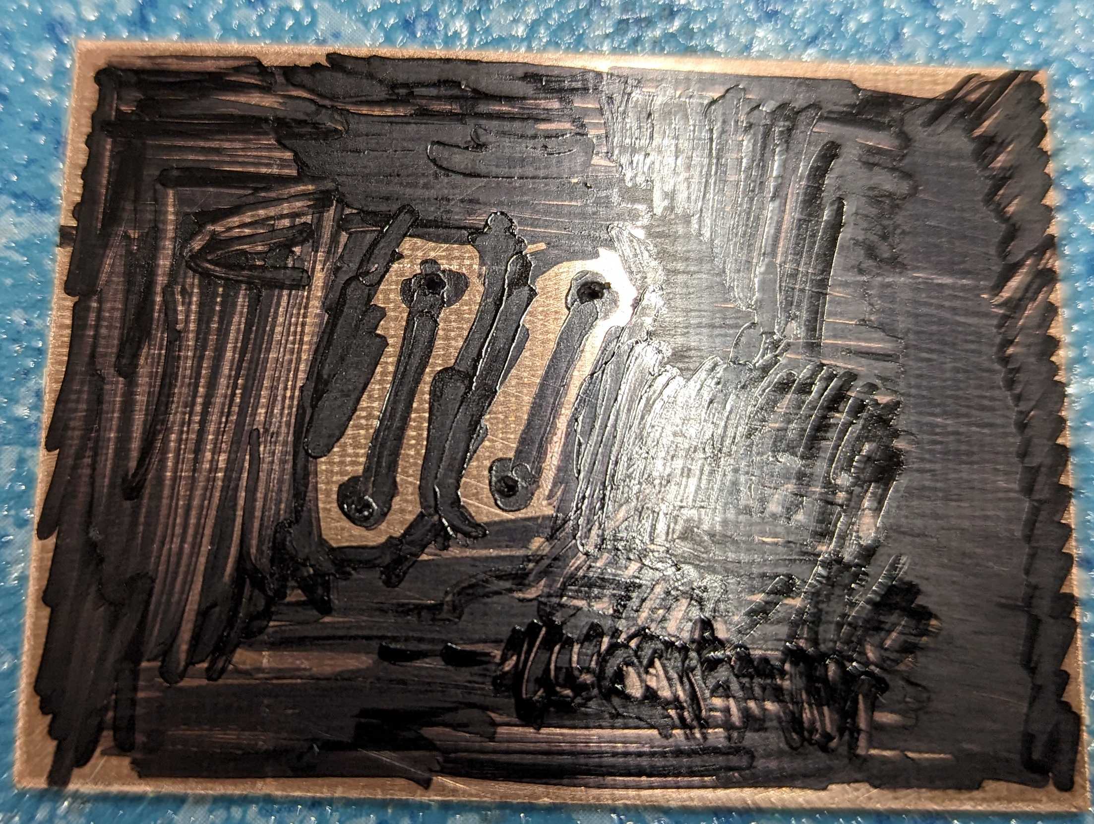
Etch the Board
Prepare an electronic scale, measuring cup, chemical-resistant shallow container and the specified PCB etchant.
⛔️DANGER
Chemical etching must be supervised in a properly equipped, ventilated workspace. Wear chemical-resistant gloves and splash goggles and follow the etchant manufacturer's Safety Data Sheet. If solution contacts the eyes or mouth, rinse immediately with clean water and seek urgent medical advice. Never use food containers again for food after chemical work.
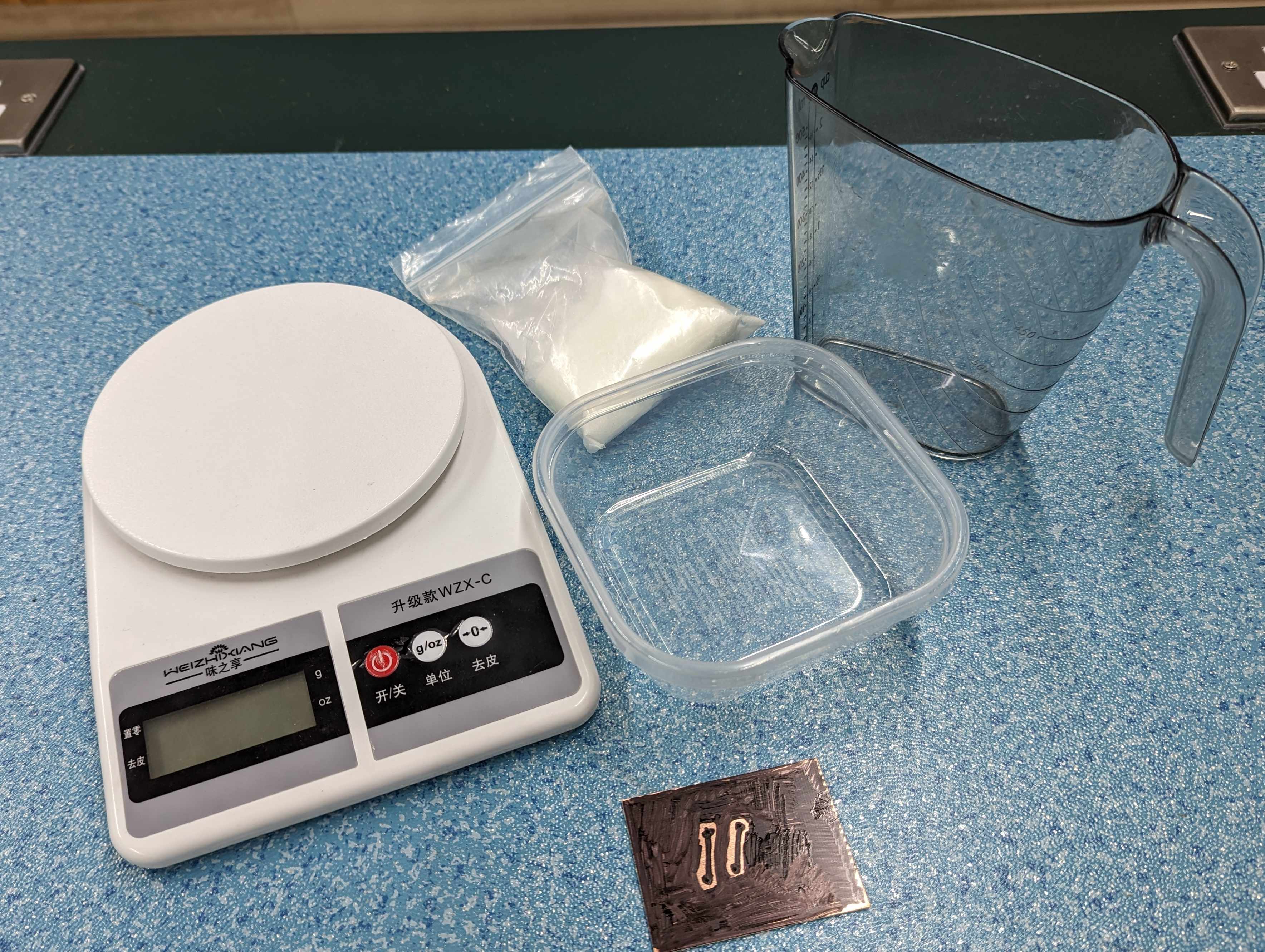
The demonstrated product uses 20 g of etching powder with 80 ml of warm water (1:4), enough to cover the board. Use the ratio and temperature specified by the actual chemical manufacturer.
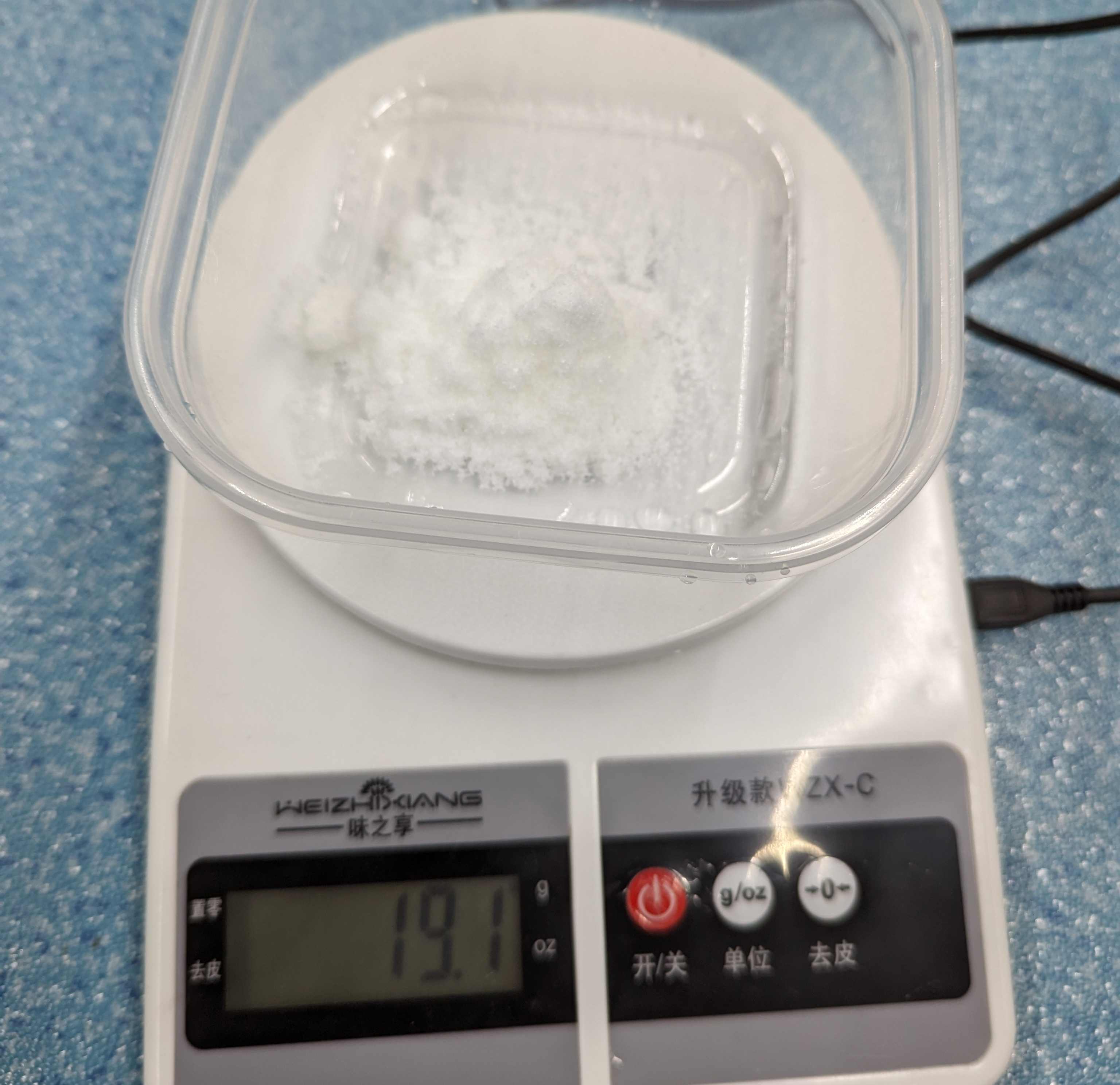
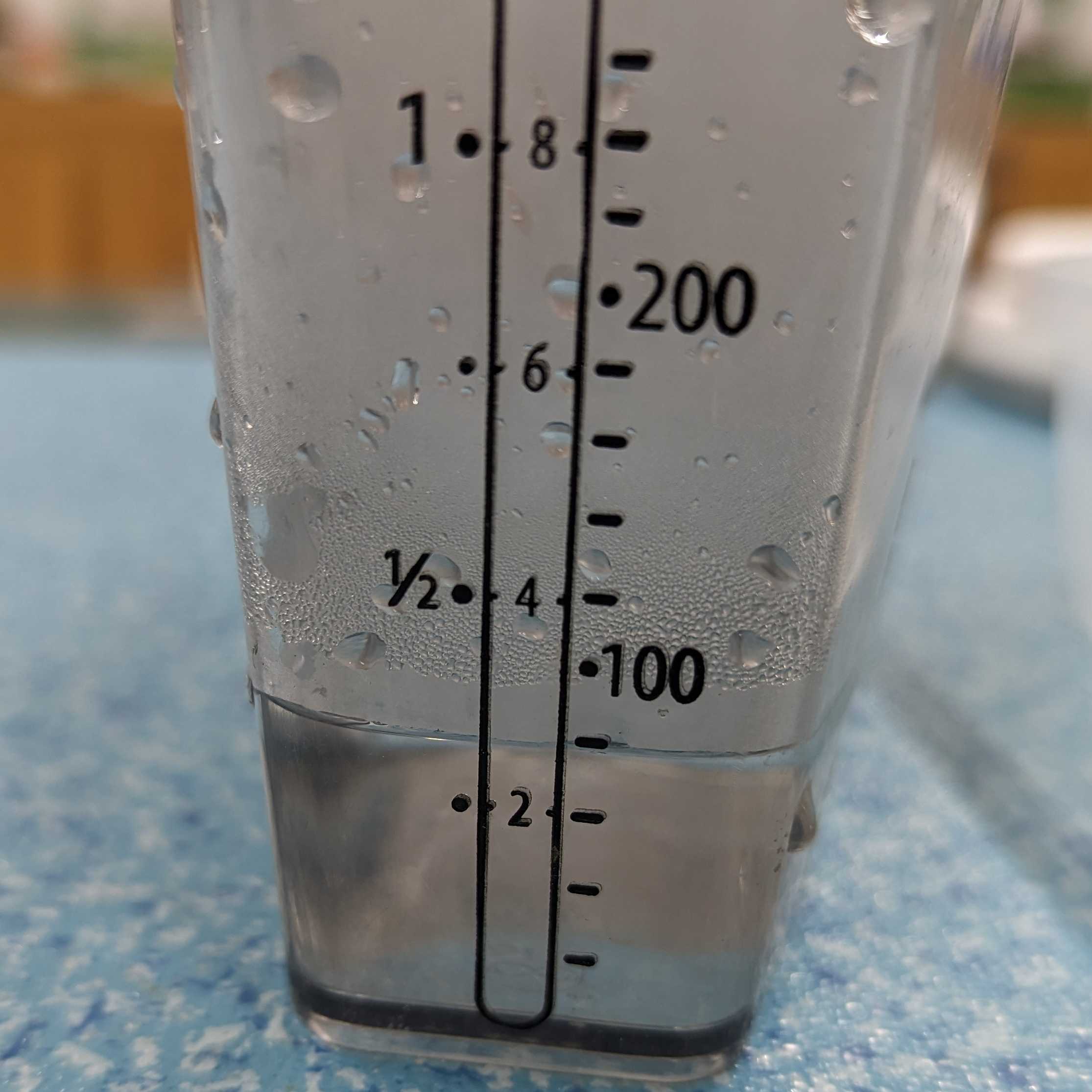
Agitate the container gently and turn the board periodically so fresh solution reaches both sides. The original demonstration uses a moving-bed 3D printer with the downloadable agitation G-code. Only use equipment in ways approved by its manufacturer and workshop supervisor; protect the printer completely from spills and fumes.
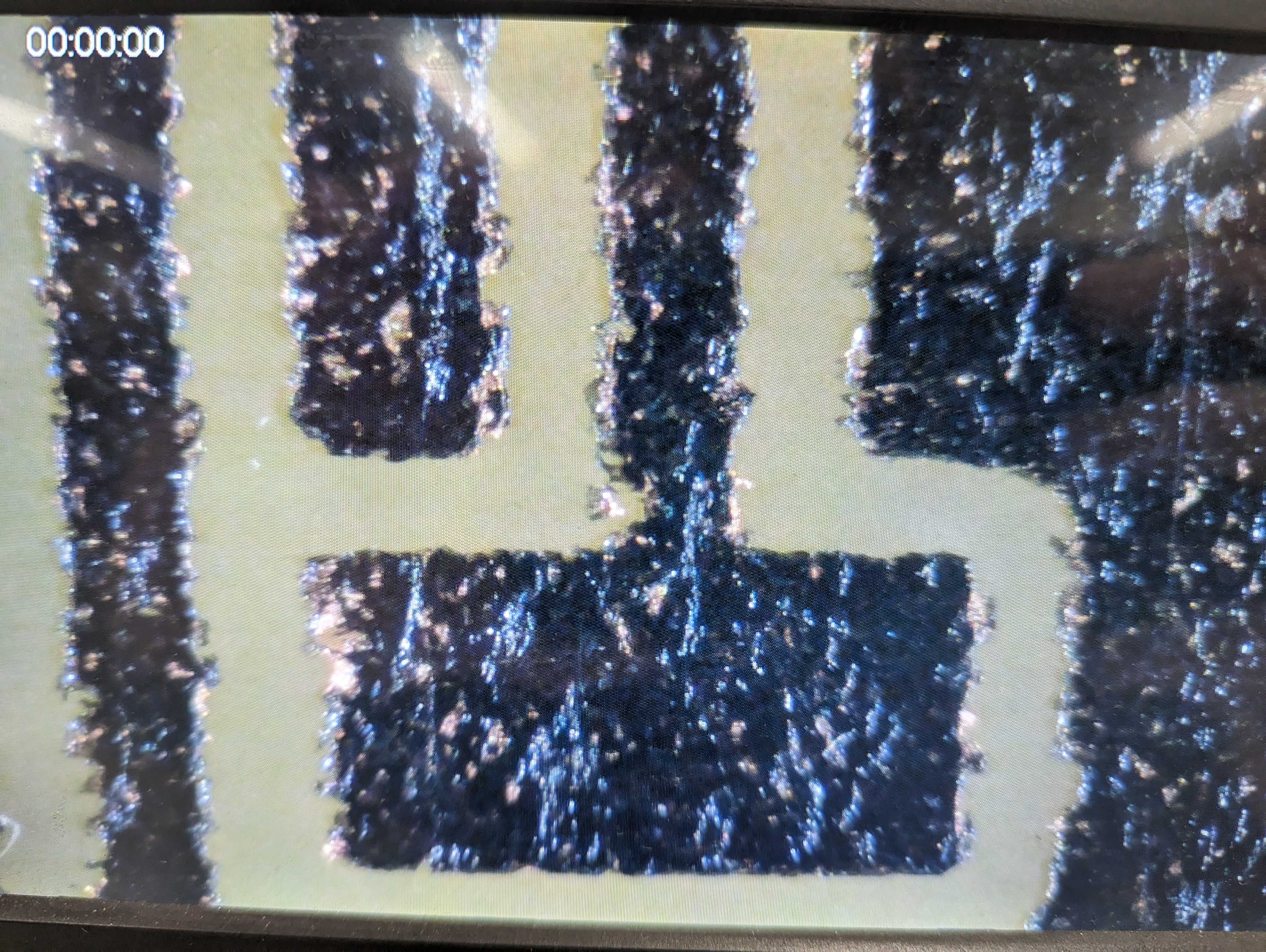
Gas bubbles can obscure the copper, so move the board gently with chemical-resistant tweezers when inspecting it. In the example, etching takes roughly 3–4 minutes; excessive time also attacks copper under the toner.
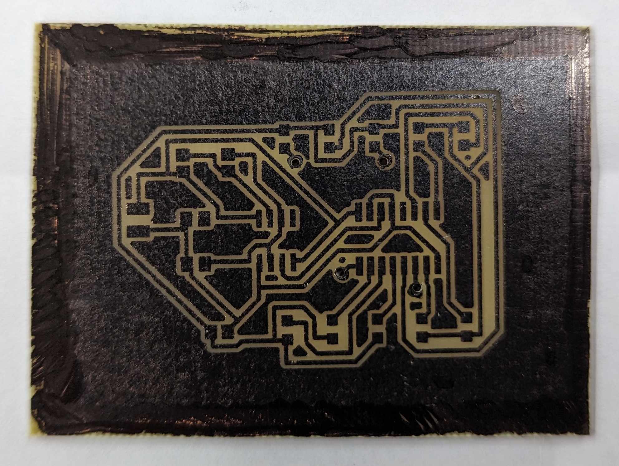
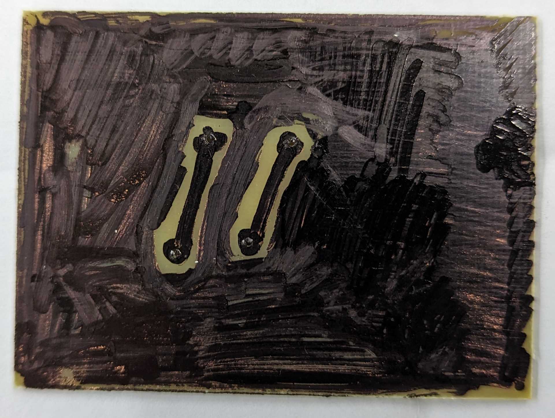
Inspect for broken tracks or copper bridges. In the example below the etch ran slightly too long, leaving some tracks thin enough to require reinforcement with solder.
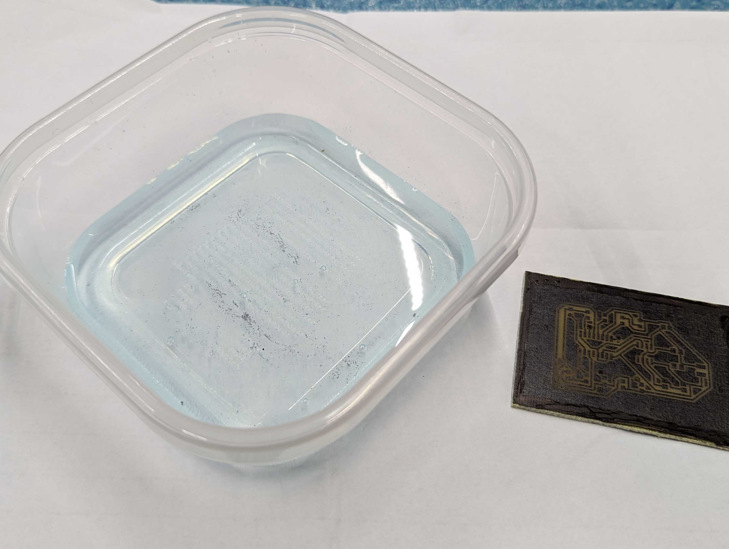
Used etchant contains dissolved copper and must be handled as hazardous waste. It may be reusable until the reaction becomes too slow.
⛔️DANGER
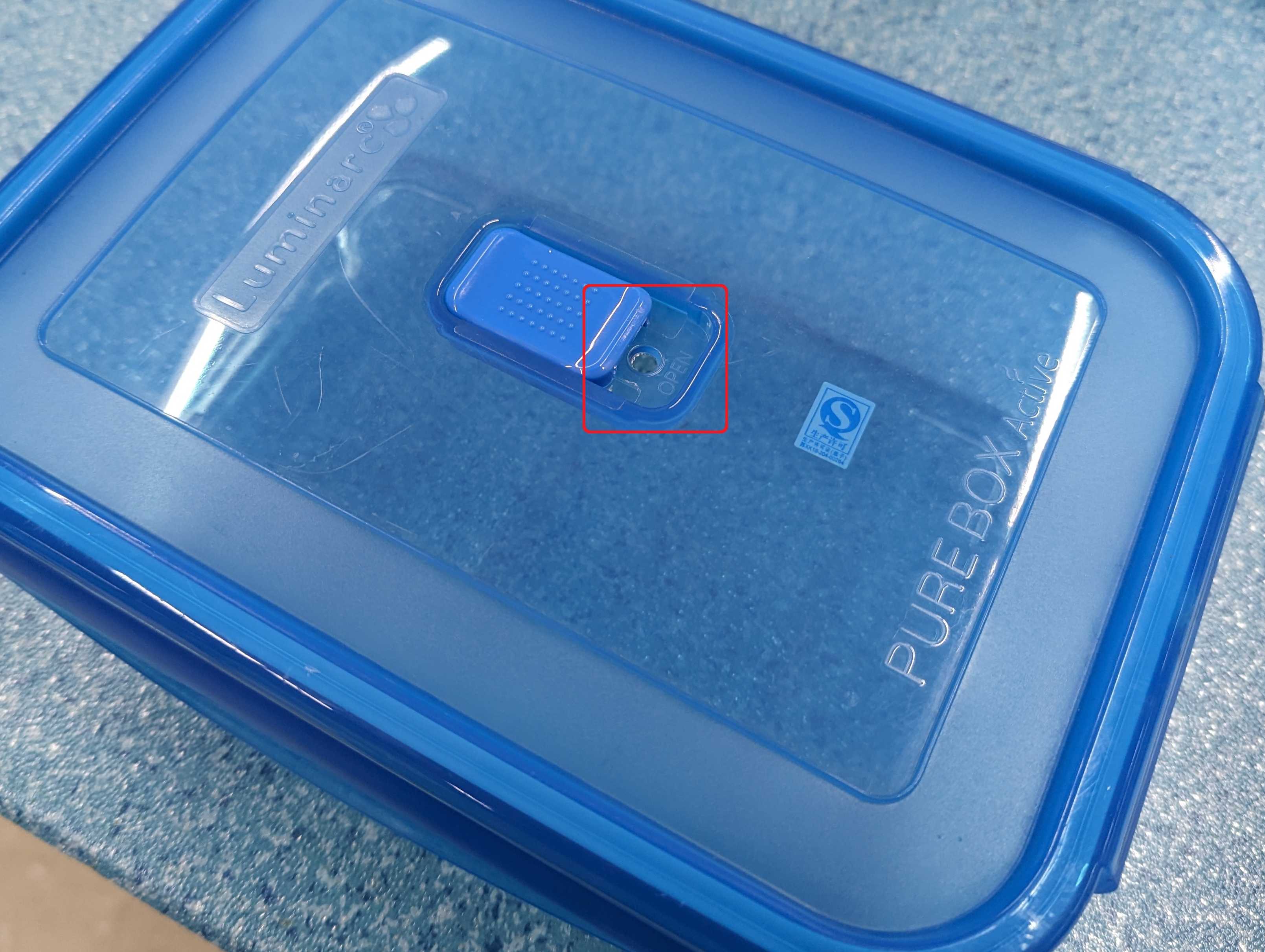
Do not pour copper-bearing etchant into a drain and do not improvise neutralisation or disposal. Store it in a compatible, clearly labelled container with the venting arrangement specified by the chemical supplier, and use your school's hazardous-waste procedure or an authorised local disposal service. Follow local regulations and the product's Safety Data Sheet.
Solder the Circuit
Commercial fabrication would apply photoimageable solder mask. For a prototype, it may be omitted. Lightly sand toner only from pads that must be soldered, leaving toner elsewhere to slow oxidation. Do not sand through the 0.035 mm copper.
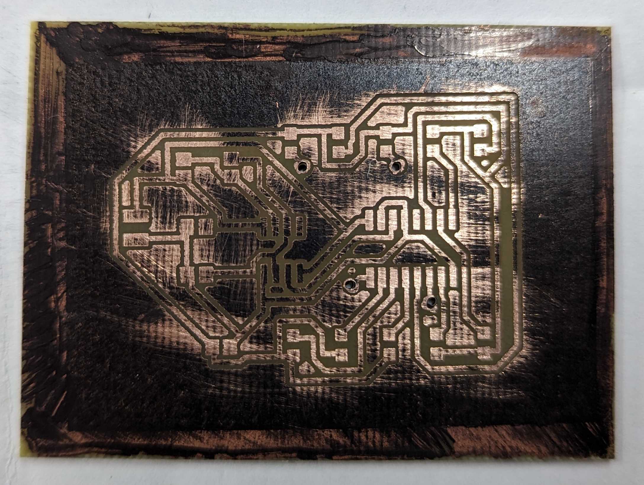
When soldering, heat both pad and lead, then feed solder into the joint—not directly onto the iron. Practise SMD soldering before working on this board and use fume extraction and eye protection.
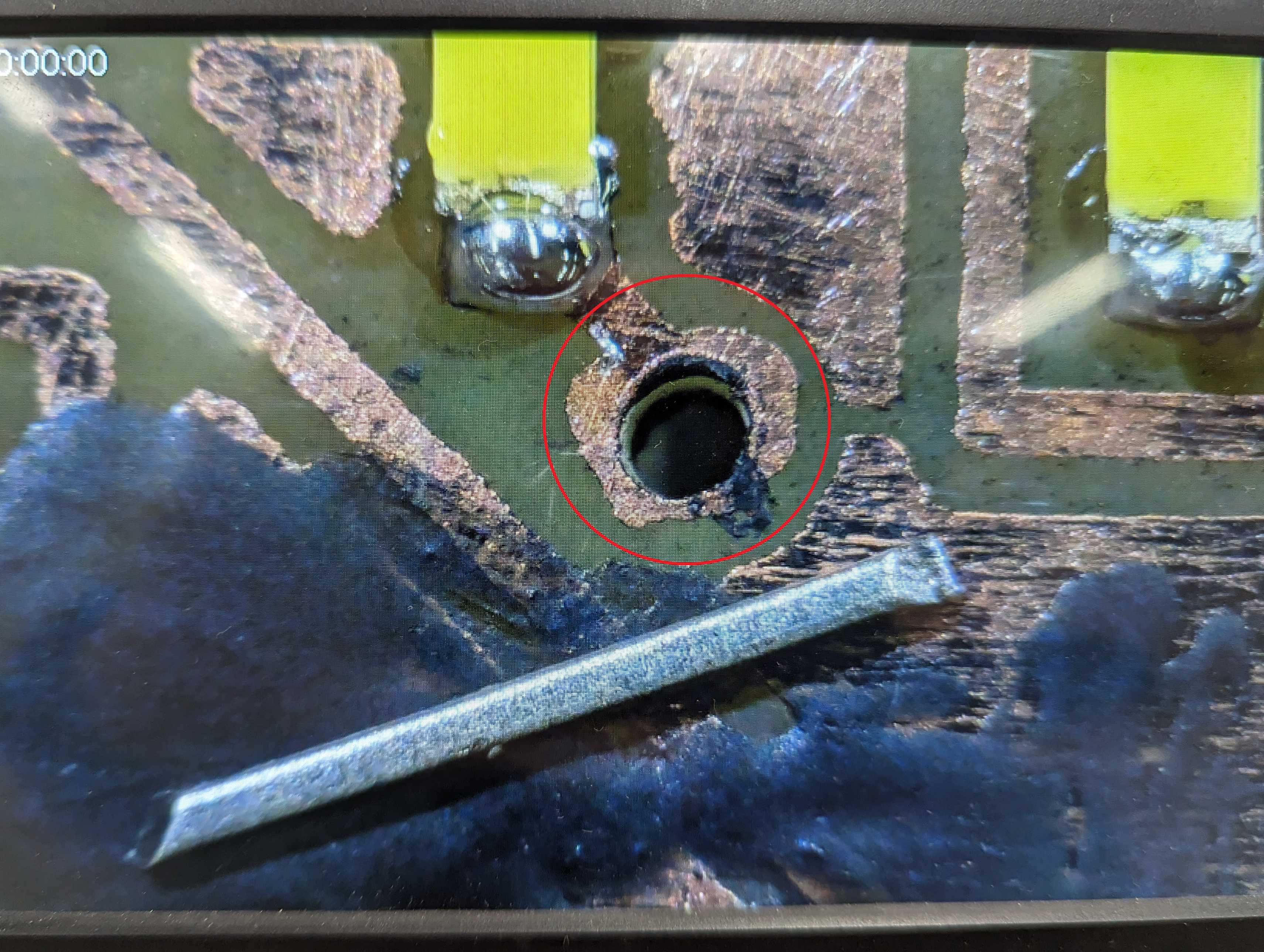
After every component is soldered, connect the top and bottom of each via with trimmed component lead or suitable wire.
Finished Result
Translation notice: This English page was generated automatically by AI and has not yet been reviewed by a human. It will be checked and revised page by page when time permits.