Drawing Schematics and PCB Layouts
We will begin with a simple 555 dimmer circuit.
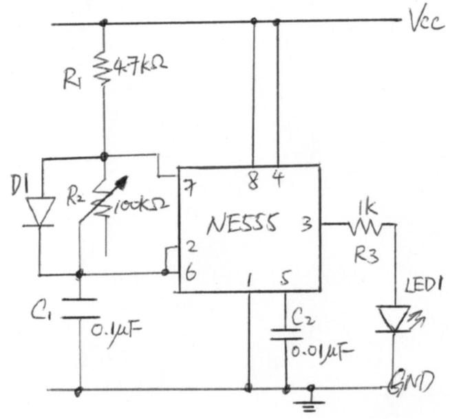
Start
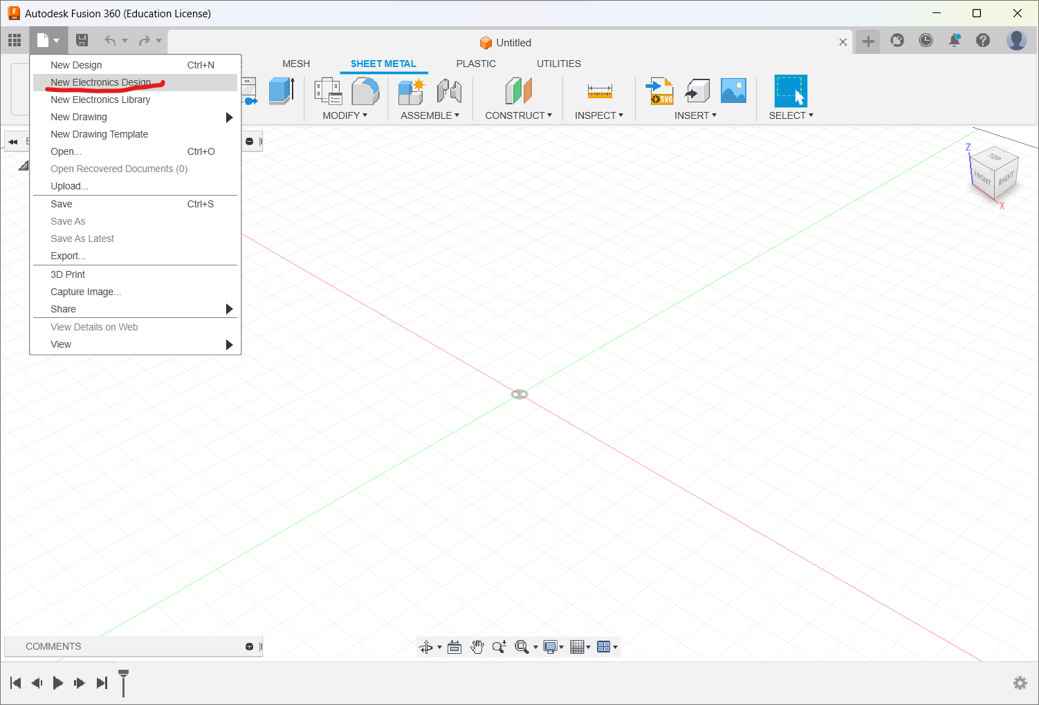
Open Fusion 360 and choose File → New Electronics Design.
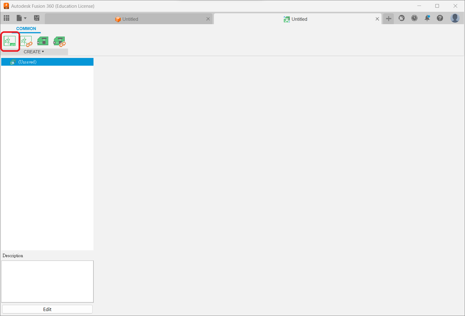
An electronics design normally contains a schematic and a physical PCB layout. It can also generate a 3D PCB model for mechanical integration. First, create a schematic from the upper-left corner of the management page.
Schematic
The left panel can be resized, detached or collapsed when it is not needed.
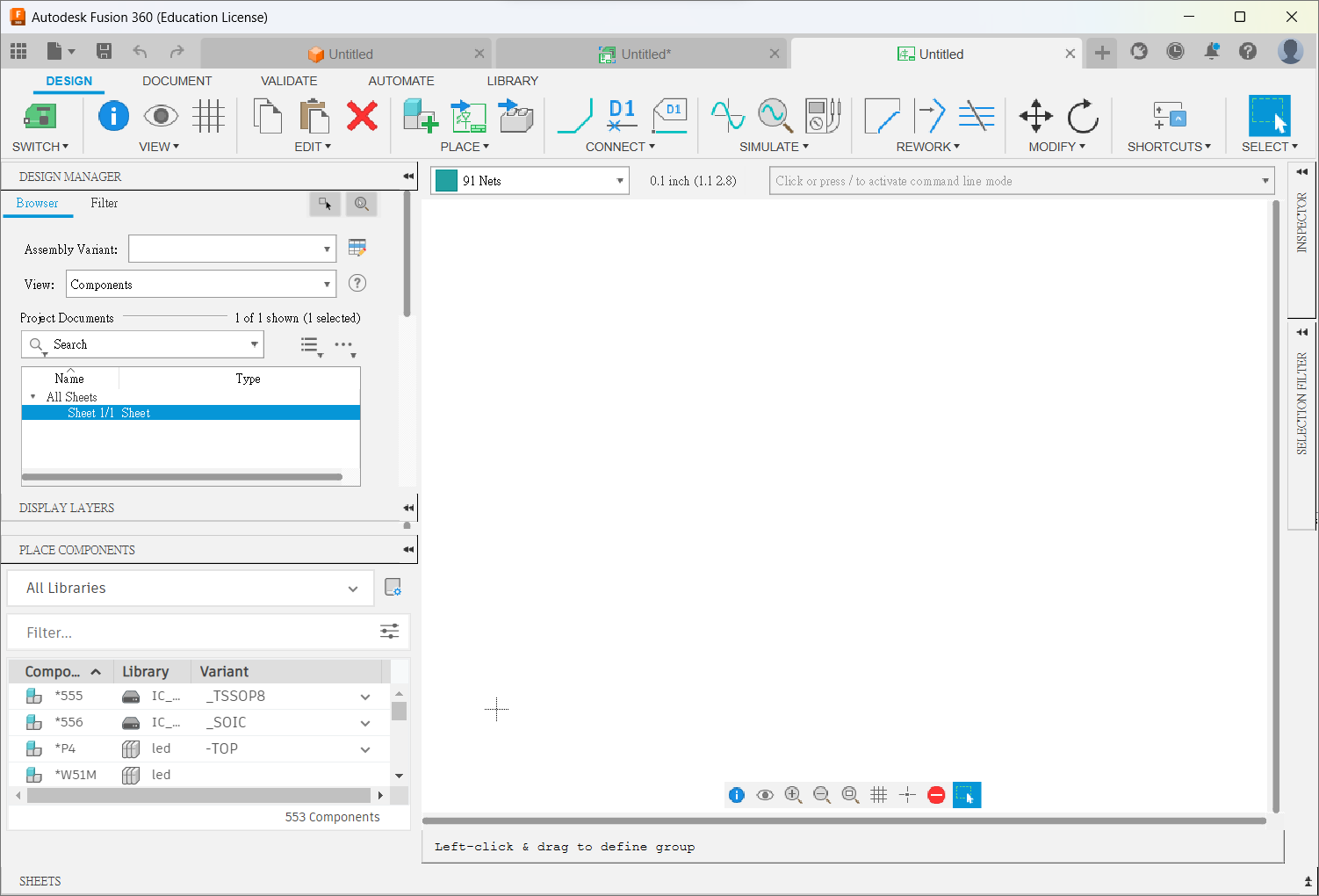
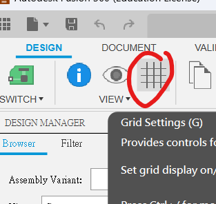
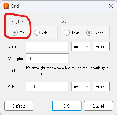
Open Grid Settings and show the grid to make alignment easier.
Add Components
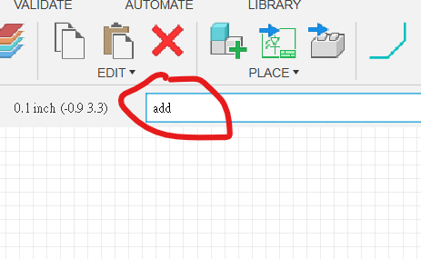
Enter add on the command line.
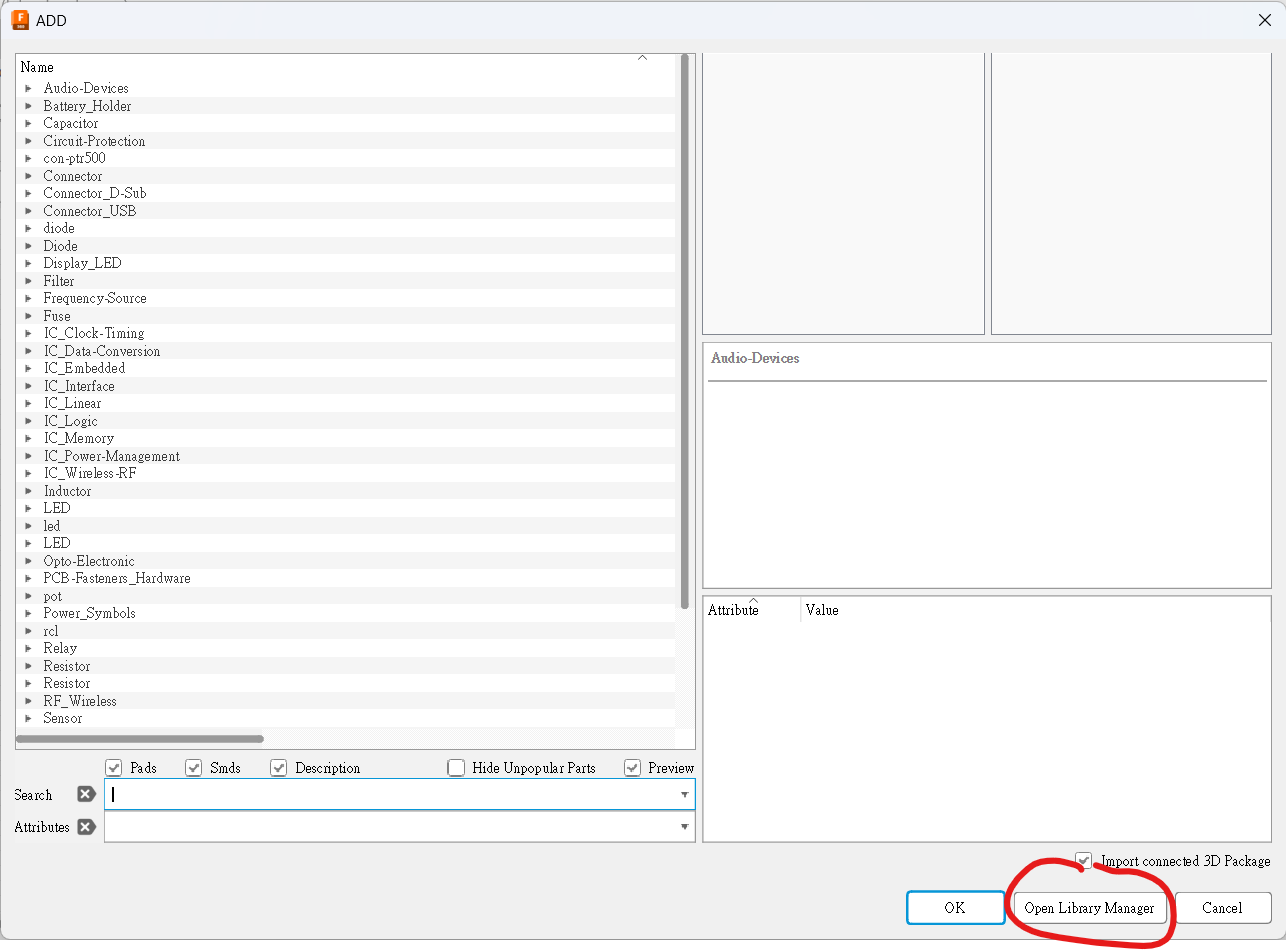
Fusion 360 does not enable every component library by default. If NE555 does not appear, choose Open Library Manager.
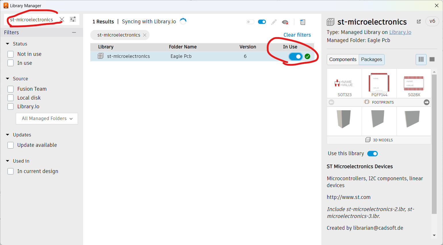
Find st-microelectronics and enable In Use.
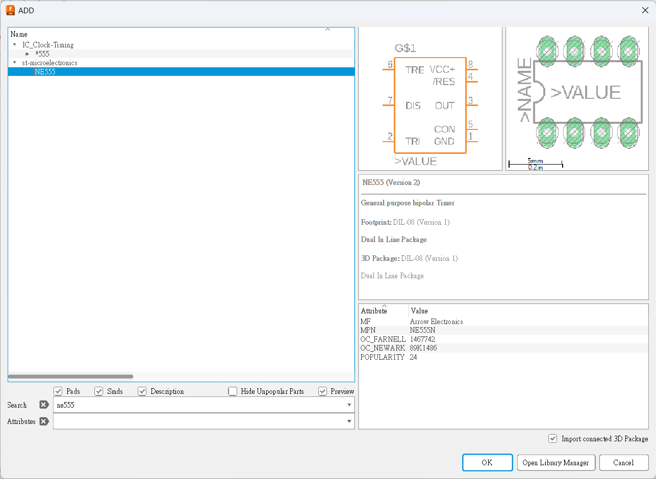
Search again for NE555, click OK and place the part.
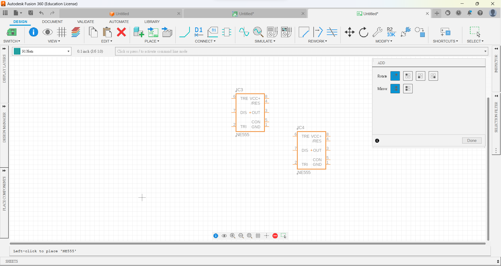
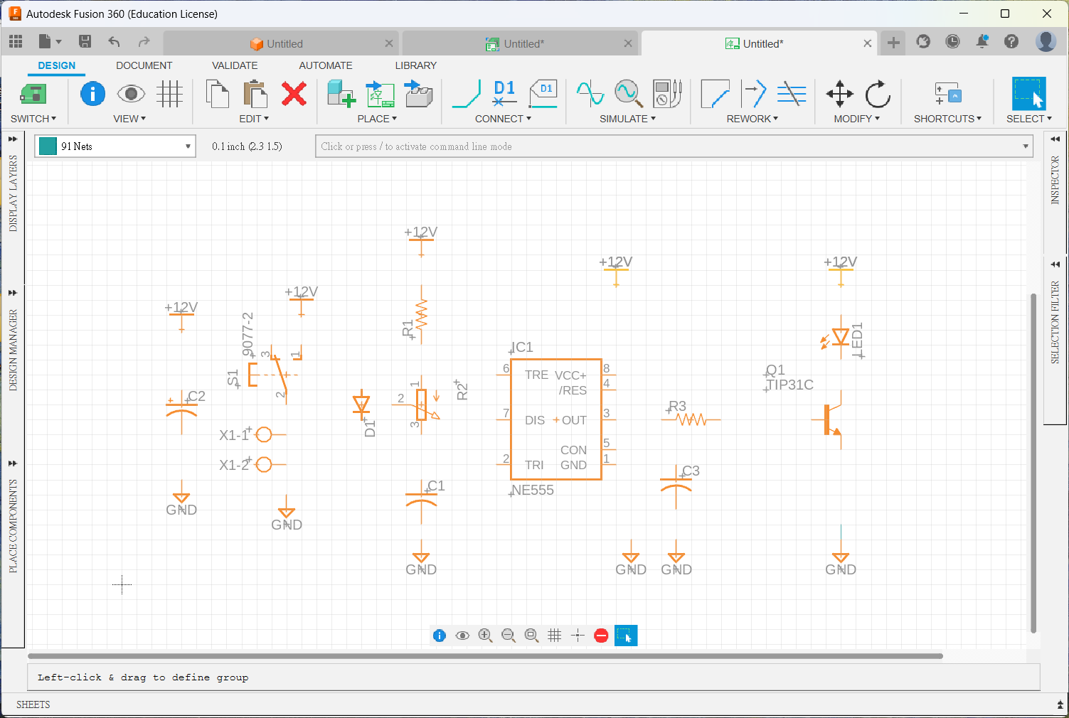
Add the remaining parts. Enable their libraries first if necessary.
| Part | Value | Device | Package | Library |
|---|---|---|---|---|
| C1 | 0.1uF | C-US025-025X050 | C025-025X050 | rcl |
| C2 | 10uF | CPOL-USE2.5-6 | E2,5-6 | rcl |
| C3 | 0.01uF | C-US025-025X050 | C025-025X050 | rcl |
| D1 | DIODE-D-2.5 | D-2.5 | diode | |
| IC1 | NE555 | NE555 | DIL-08 | st-microelectronics |
| LED1 | LED3MM | LED3MM | led | |
| Q1 | TIP41C | TIP31C | TO220 | transistor-npn |
| R1 | 4.7k | R-US_0207/2V | 0207/2V | resistor |
| R2 | 100k variable | 3RP/1610N | 3RP/1610N | pot |
| R3 | 1k | R-US_0207/2V | 0207/2V | resistor |
| S2 | 9077-2 | 9077-2 | 9077-2 | switch-misc |
| VIN | AK500/2 | AK500/2 | con-ptr500 | |
| +12V | +12V | supply1 | ||
| GND | GND | supply1 |
Use Move to position parts, right-click while moving to rotate, Copy to duplicate, Name for reference designators and Value for component values.
ℹ️INFO
To move several parts together, select them with Group, start Move, then right-click the highlighted group and choose Group: Move.
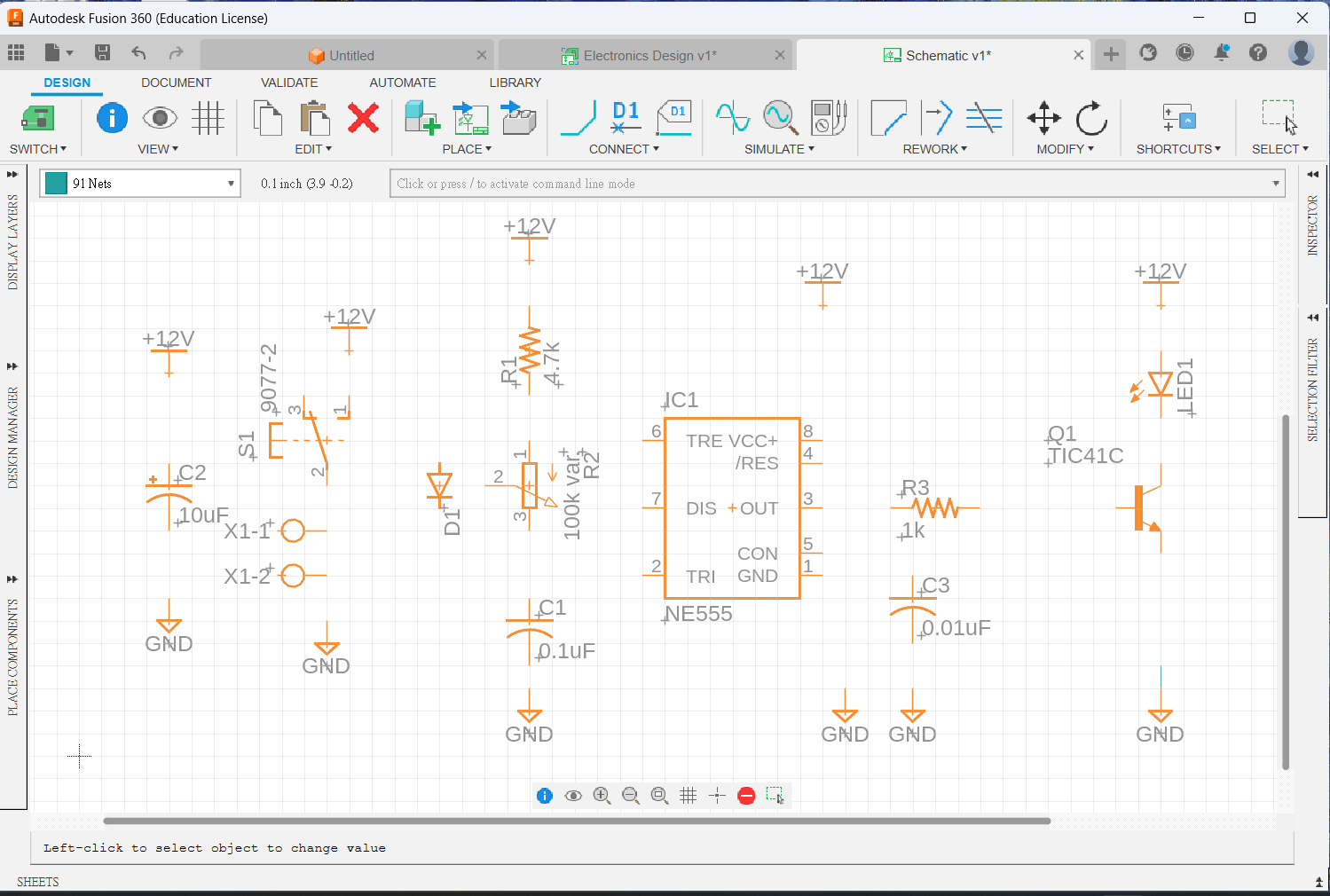
Connect Components
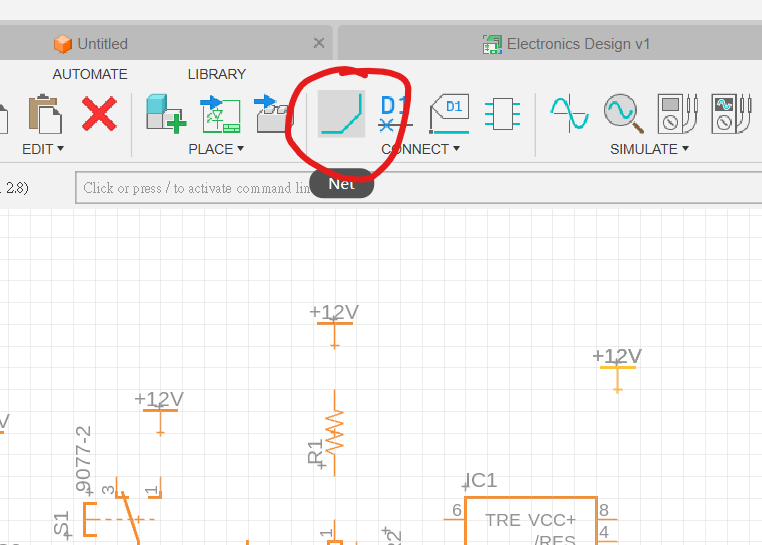
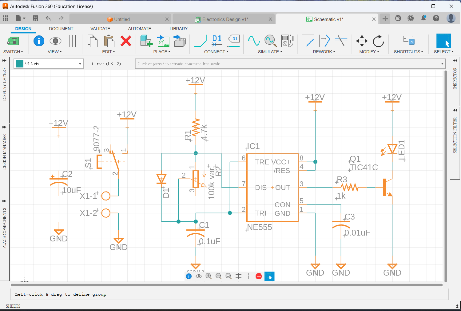
Use Net to connect pins. Right-click while drawing to change the bend direction, or choose a wire shape in the toolbar.
💡TIP
When crossing nets must connect electrically, place a Junction dot. A crossing without a junction is not a connection.
Electrical Rule Check (ERC)
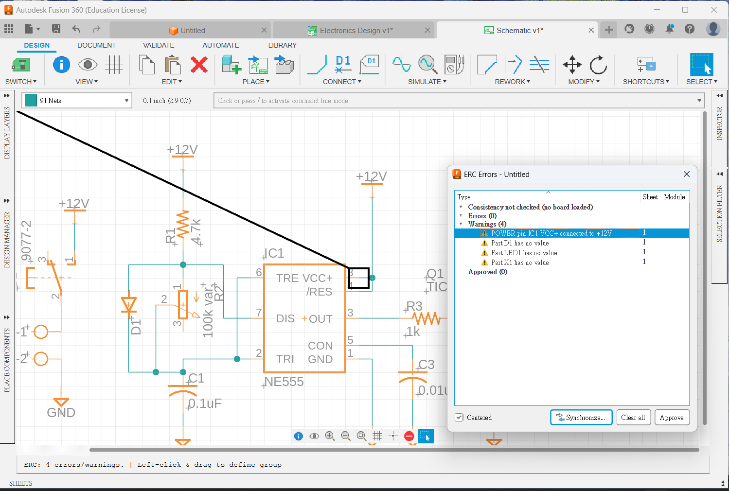
Enter ERC. Review every result. Warnings often indicate a missing value and may be approved after inspection, but all errors must be corrected. Common errors include a missing junction, a net that only appears to touch a pin, and omitted connections.
PCB Layout
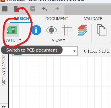
Click the small white/green SWITCH icon in the toolbar to create or open the PCB layout.
Preparation
The parts appear beside the board outline. Thin airwires represent the electrical connections defined in the schematic.
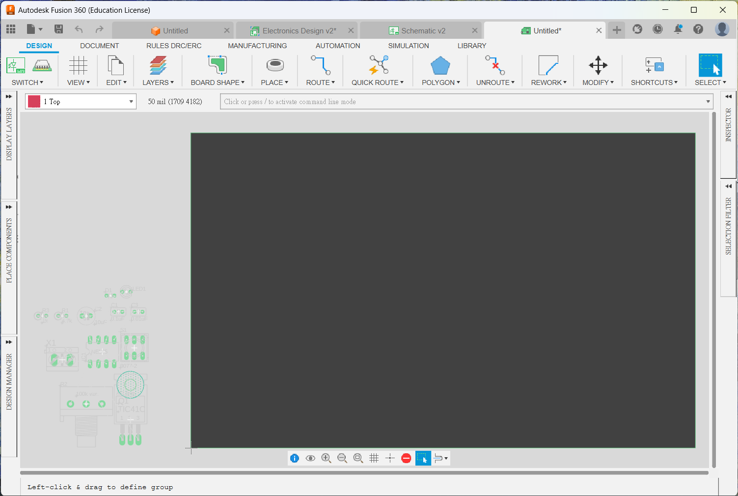
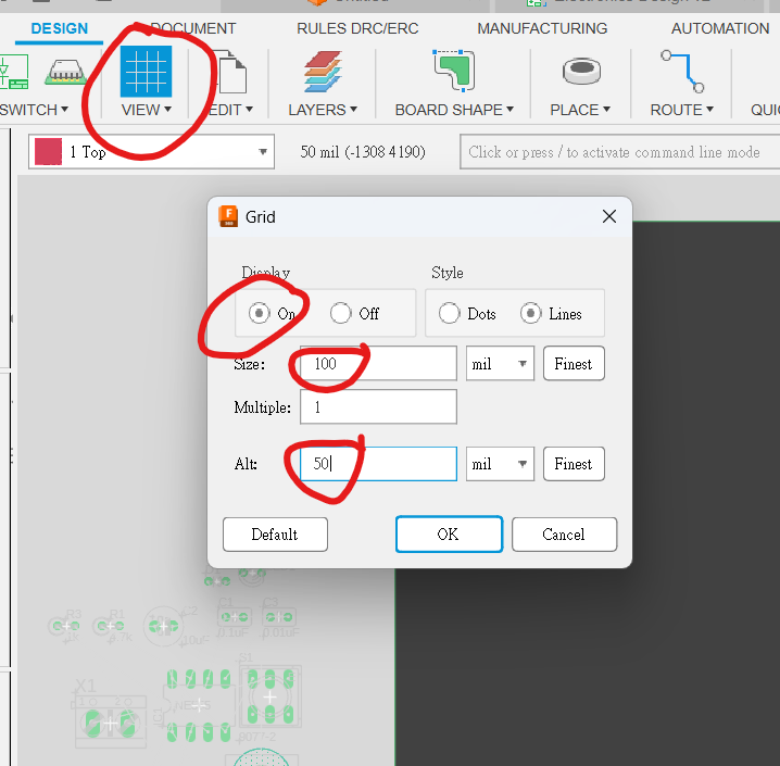
Open Grid, set Display to On, Size to 100 mil and Alt to 50 mil. Movement follows the 100 mil grid; holding Alt temporarily uses 50 mil.
ℹ️INFO
100 mil is 0.1 inch, or 2.54 mm: the standard pitch of breadboards and many through-hole components. PCB layouts therefore often use mil rather than millimetres.
Place Components
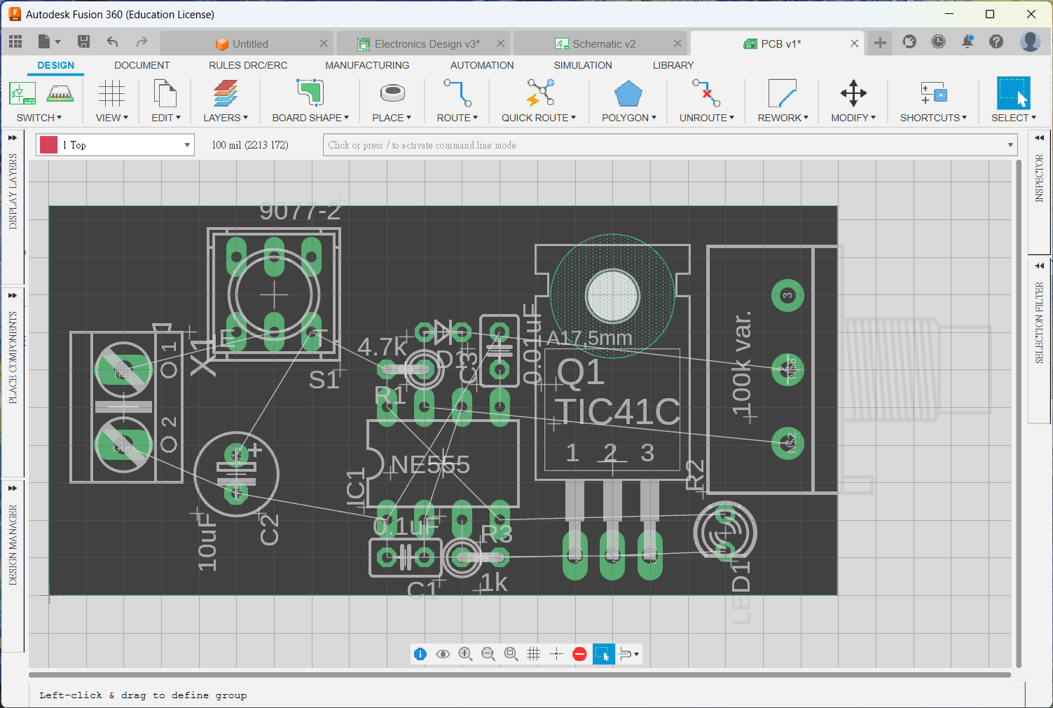
- Resize the green board outline approximately.
- Use
Moveto place components. - Right-click while moving, or use
Rotate, to rotate them. - Middle-click, or use
Mirror, to move a component to the bottom side. This example keeps every component on top. - Follow the airwires and orient related parts so that connections are short and uncomplicated.
Design Rules
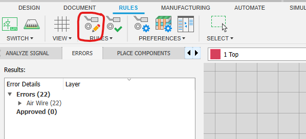
Open Rules → Design Rules.
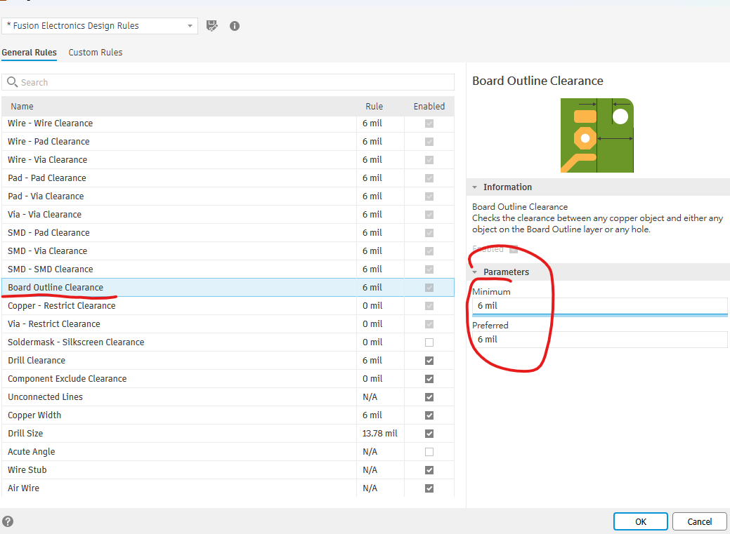
Under Board Outline Clearance, reduce the default 40 mil clearance to 6 mil for this factory-made board.
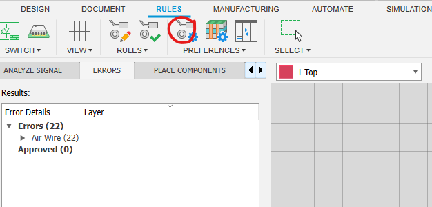
Open Design Preferences, then the Masks page.
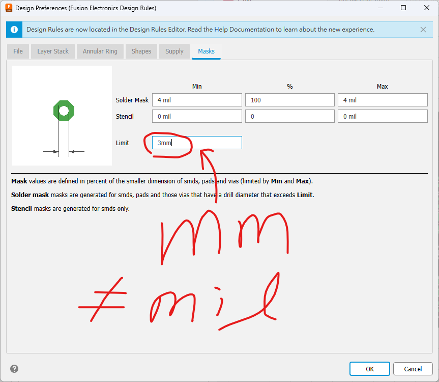
The upper settings define solder-mask expansion around pads. Limit determines which holes are large enough to remain uncovered; set it to 3 mm.
⚠️WARNING
Include the mm unit explicitly; the default unit is mil.
📝NOTE
At 0 mil, every via is exposed, which makes accidental solder bridges more likely.
Autoroute
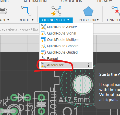
Click the autorouter icon.
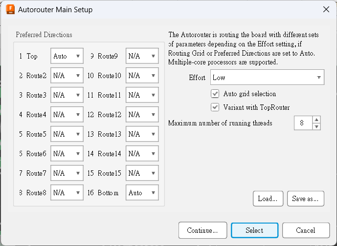
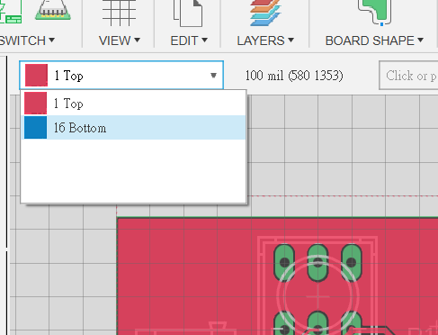
Layers 1–16 represent available copper layers. This is a two-layer board, so route only 1 Top and 16 Bottom, then click Continue.
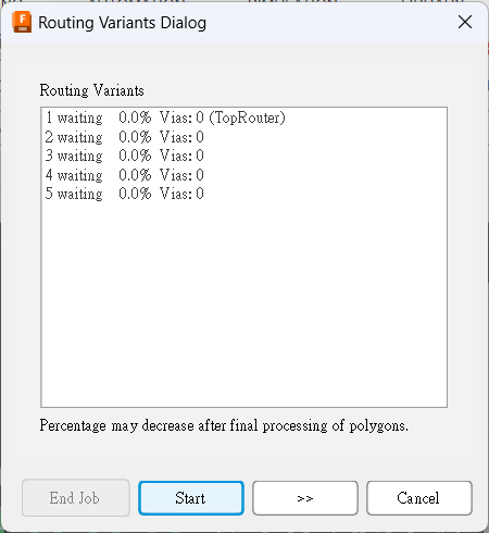
Click Start. The router tries several strategies; the first result is generally the most optimised and may take longer.
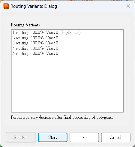
⛔️DANGER
Do not accept the routing until it reports 100% completion.
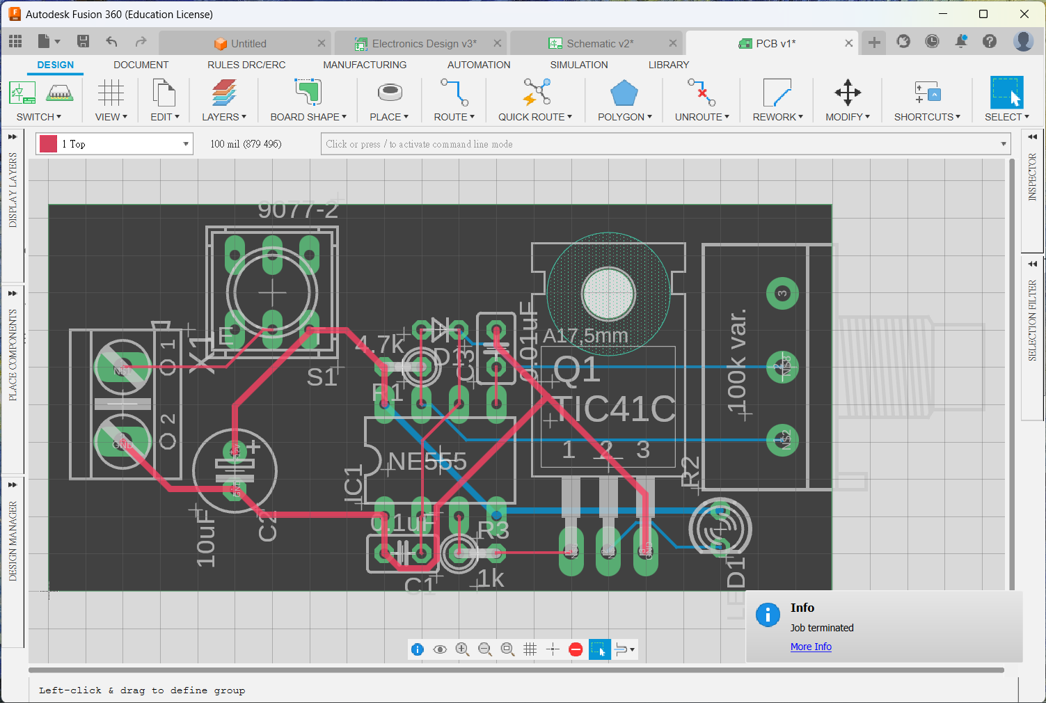
Copper Polygon
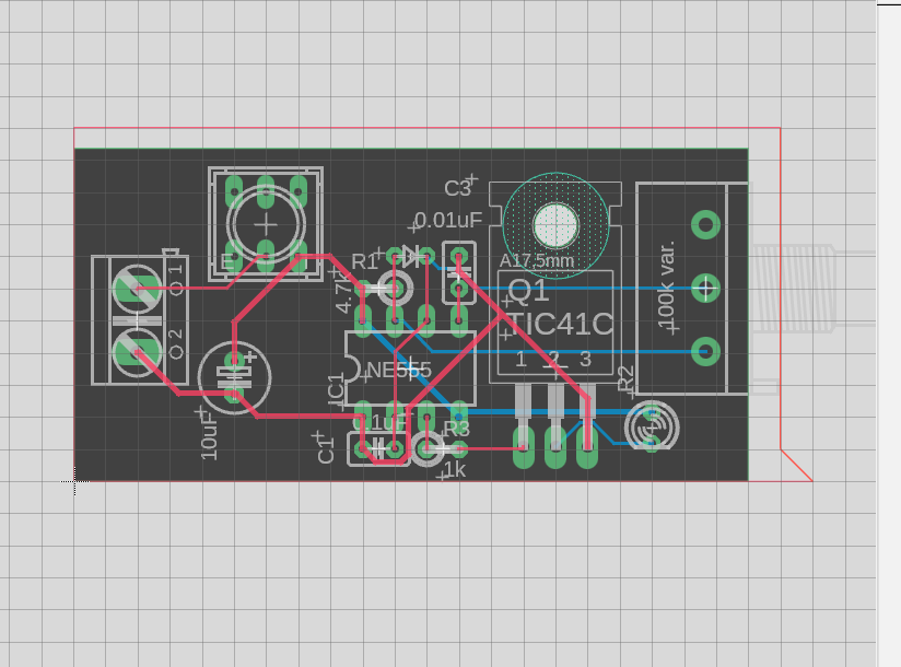
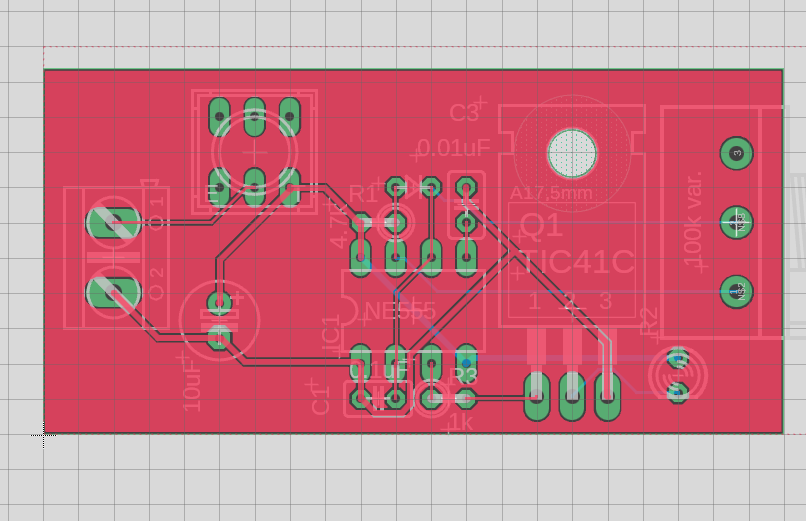
A PCB begins as copper-clad laminate. Removing very large copper areas takes longer and can undercut thin tracks. A polygon keeps unused copper and etches only the isolation around tracks.
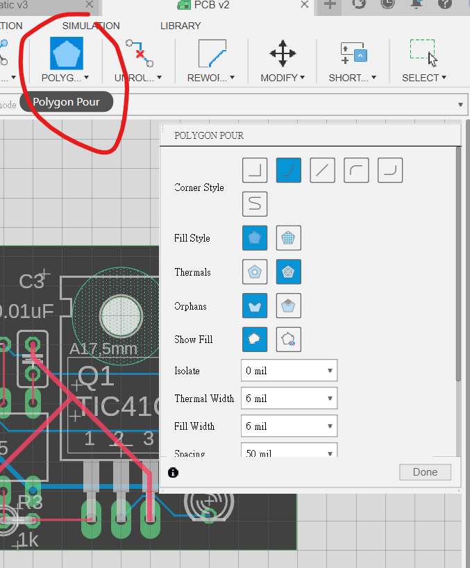
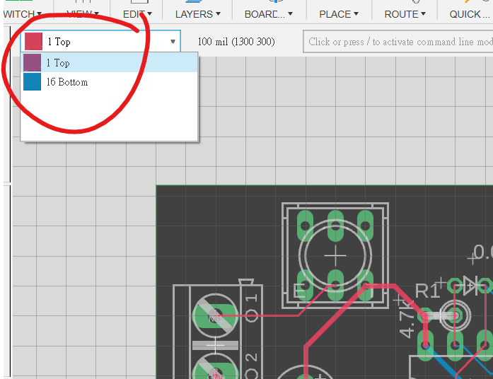
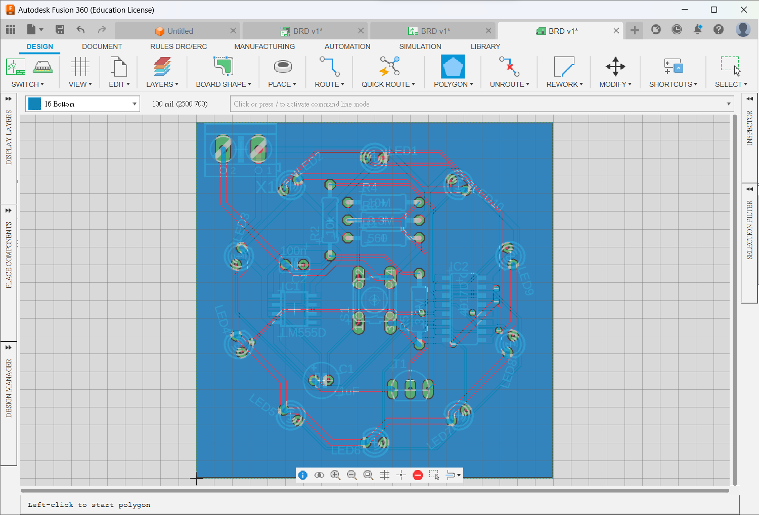
- Select
Polygonor enterpolygon. - Choose
TOPin the toolbar and keep the other settings at their defaults. - Draw a rectangle around the board outline.
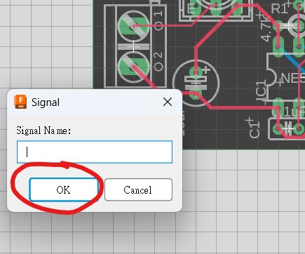
- When asked which signal to connect, leave it blank for this exercise and click
OK. In practical boards, polygons are often assigned to a power or ground net.
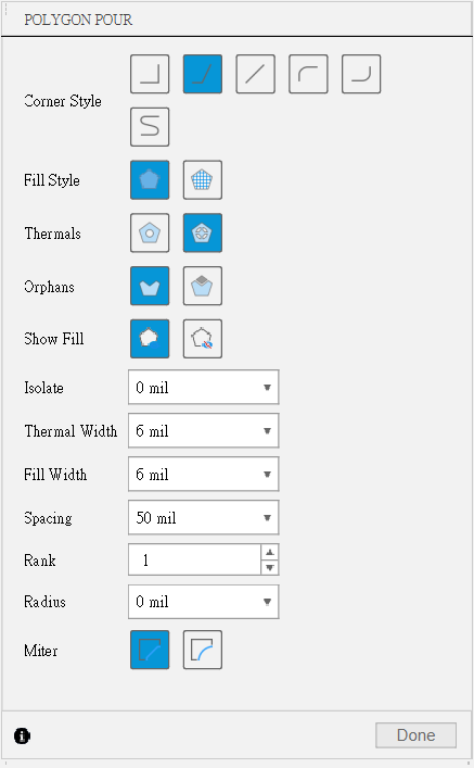
Repeat for the bottom layer.
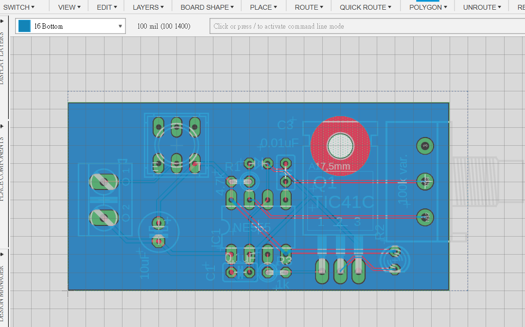
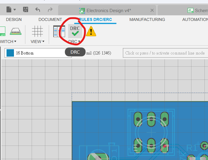
Design Rule Check (DRC)
Run DRC after routing and pouring copper. A clean result may produce no dialog; otherwise, inspect and correct every error.
Workflow Summary
- New Electronics Design
- Schematic: add parts and set names/values.
- Nets: connect pins and add Junction at connected crossings.
- ERC: fix every error; approve only understood warnings.
- Switch to PCB: set the 100/50 mil grid and place parts.
- Rules: set required clearance and a 3 mm mask limit.
- Autoroute: reach 100% completion.
- Polygon: pour copper on top and bottom.
- DRC: verify physical clearances and connectivity.
- Output: export Gerber files for manufacturing.
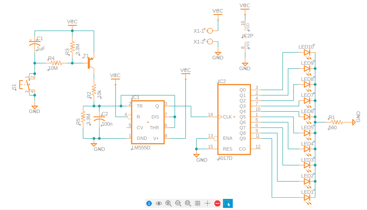
Exercise 1: 555 + 4017 LED Roulette
💡TIP
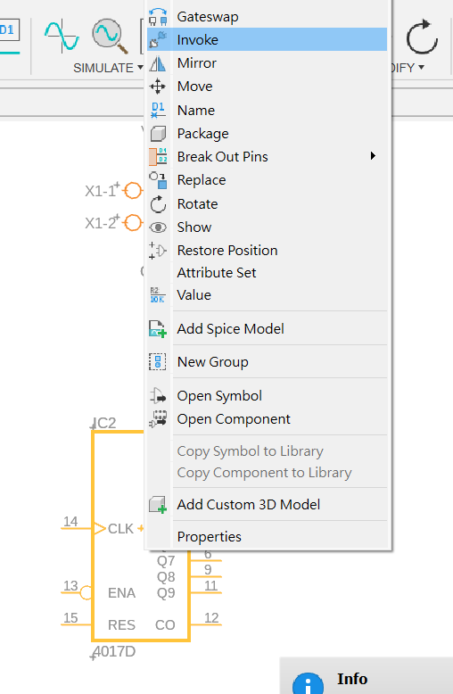
Pins 16 and 8 of the 4017 are hidden by default. Right-click the 4017, choose Invoke, and expose those power pins.
Showing hidden IC power pins
Some libraries hide power pins that normally connect to VCC or VDD. Use Invoke as shown:
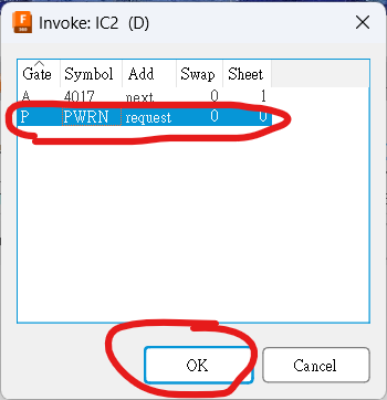
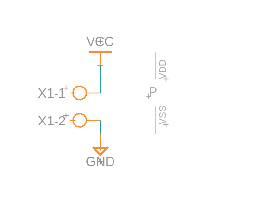
Choose R1 between 330 Ω and 1.5 kΩ according to the supply voltage. Use the following parts:
| Part | Value | Device | Package | Library |
|---|---|---|---|---|
| C1 | 1uF | CPOL-USE2-5 | E2-5 | rcl |
| C2 | 100n | C-US025-024X044 | C025-024X044 | rcl |
| IC3 | LM555D | LM555D | SO08 | linear |
| IC2 | 4017D | 4017D | SO16 | 40xx |
| LEDs | LED3MM | LED3MM | led | |
| R1 | 560 | R-US_0207/10 | 0207/10 | rcl |
| R2 | 10K | R-US_0207/10 | 0207/10 | rcl |
| R3 | 3.3M | R-US_0207/10 | 0207/10 | rcl |
| R4 | 10M | R-US_0207/10 | 0207/10 | rcl |
| R5 | 3.3M | R-US_0207/10 | 0207/10 | rcl |
| S1 | 10-XX | B3F-10XX | switch-omron | |
| T1 | BC557A-PNP-TO92-EBC | TO92-EBC | transistor | |
| X1 | AK500/2 | AK500/2 | con-ptr500 |
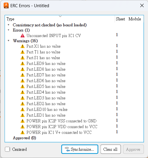
The expected ERC warnings may be approved after review; any additional errors indicate a real design issue.
PCB Layout
Use Arrange to place the ten LEDs in a precise circle:
- Set the outline to
2000 × 2000 mil. - Select all ten LEDs and enter
arrange. - Choose a circular array centred at
(1000, 1000) mil, with a90°starting angle and800 milradius.
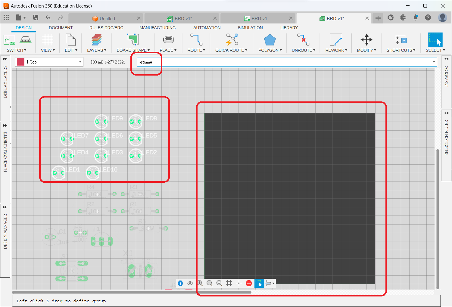
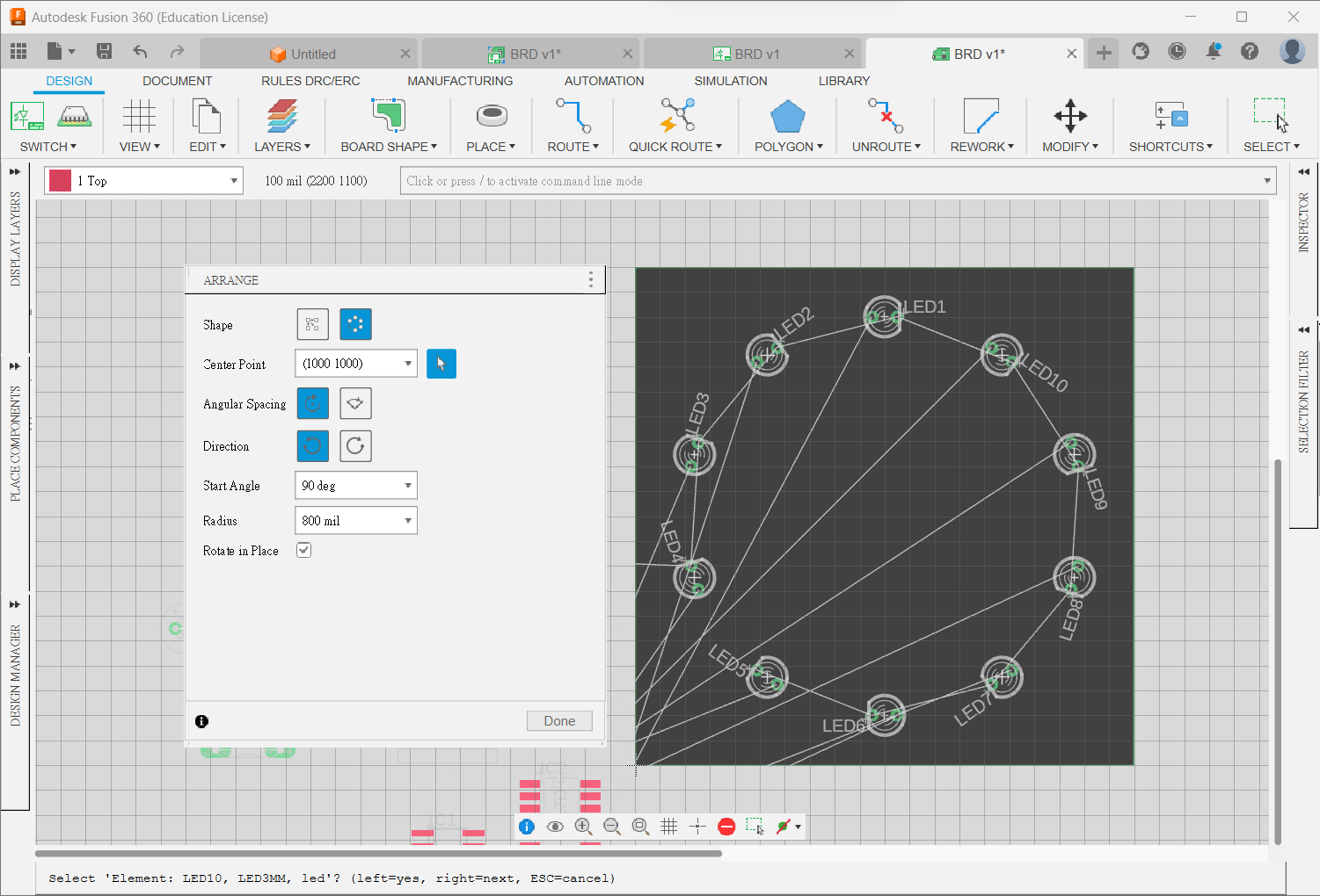
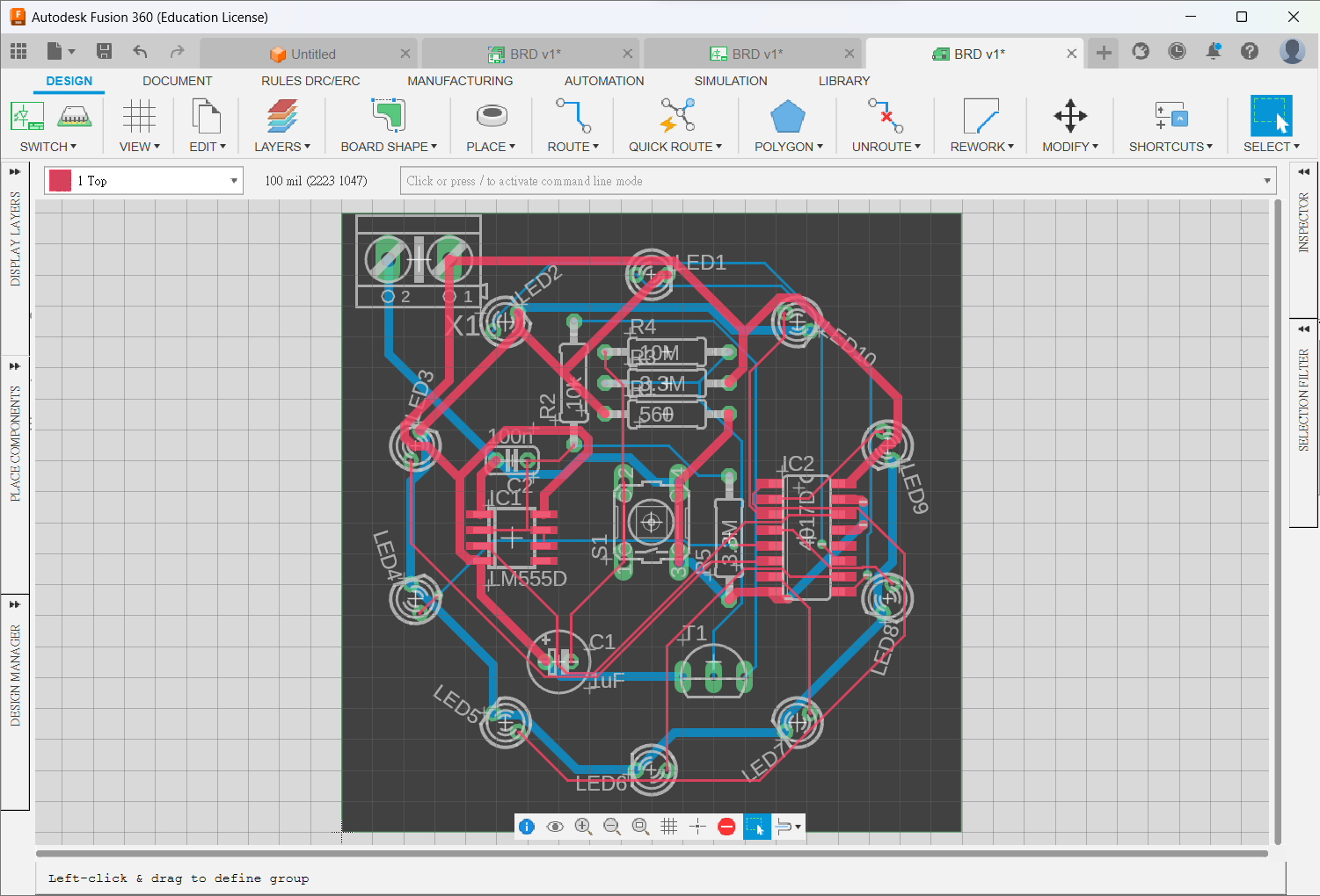
Place the power connector near the outside and the button in the centre. Set the board-outline distance to 6 mil, mask limit to 3 mm, complete the routing and add polygons.
Translation notice: This English page was generated automatically by AI and has not yet been reviewed by a human. It will be checked and revised page by page when time permits.